Close
0%
0%

Project Ember

Homebrew Retro-Inspired 32-bit CPU And Video Game System

tomTom
Public Chat
Similar projects worth following
Project Ember is an evolving long-term research project. The plan is to develop a homebrew CPU, GPU, and ultimately video game system and teaching tool for anyone interested in the intricacies of video game development software and hardware. Drawing inspiration from early home video game systems and computers like the Atari 2600, Colecovision, Nintendo NES, as well as early home computers such as the Atari 800, Commodore 64, and Amiga, Ember embraces the technology of the time, but with a nod to features of more modern game systems with a 32-bit architecture, larger memory space, and modern development tools including LLVM compiler integration and source-level debugger.

The idea for Project Ember came about while watching YouTube videos of all the awesome projects people were doing with breadboard-based computers using 6502 and 6800 CPUs, arcade emulators running in hardware on FPGAs, and old conference videos from Hackaday, GDC (Game Developer Conference), and many local hacker gatherings. The kicker was watching Ben Eater and his videos on 6502 and discrete circuit breadboard computers, timing circuits, and more. He explains things in a way that all the years of formal learning didn’t, this is where it finally clicked.

From there it was just a matter of learning everything there was to know about game and computer system design, programming, and implementation, both in software using emulation and in hardware. Once I felt I had a grasp on how I might accomplish the task, I began researching previous CPU and GPU designs (Though in our case retro ‘GPU’s are more like video chips than what we think of modern GPUs), learning the details of each and every home video game console and computer of the 1970s and 80s, as well as many of the arcade boards of the time. 

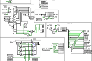
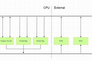
Armed with this newfound knowledge, I set out to design my first CPU. I made some initial executive decisions, like 32-bit, little-endian, load/store RISC architecture, etc. Some of these decisions, like 32-bit, are more for ease of development than historical accuracy, since programming in assembly on 8-bit CPUs was not done for fun back in the day, but because there was no other option for low-cost hardware. If the people programming for the Atari 2600 could have done so on a 32-bit CPU, I’m certain they would have as well! Once I had the basic instruction set designed, I created a very simple assembler and emulator for the CPU to test it out in theory.

The next logical step was to design a video chip. I decided to go with something very similar to the TI 9918 (as many of the systems of the time did) with various tiled display modes and some sprites. Also, since each display mode is a separate entity, I could just implement one at a time, the first being a 80x44 tiled text mode with a 16x16 character 1-bit font containing up to 256 tiles. The first half of the initial font tileset was text and special characters, leaving the second half for graphics characters and other things. Later, I added sprites and other modes which allowed for moving objects on the screen, color tilesets, and scrolling or rotating backgrounds.

With a basic CPU and GPU implemented in the emulator, I next added an interrupt controller and IO support. This allowed keyboard and gamepad input. Keyboard support meant I could write a basic monitor program to display memory values or run programs, basically allowing interactions with the machine when running in the emulator.

At this point, I had the basics needed to implement simple applications and games, albeit without sound. However, my simple assembler was not up to the task. After some additional research, I decided to implement a native back-end assembler for Ember32 assembly language in LLVM. There were other suites I could have used, like gcc, however, longer-term I wanted to be able to write higher-level language applications for the system. Not only C/C++, but also RUST, Swift, or any number of others. These languages are primarily supported on LLVM, so that is what I decided to use.

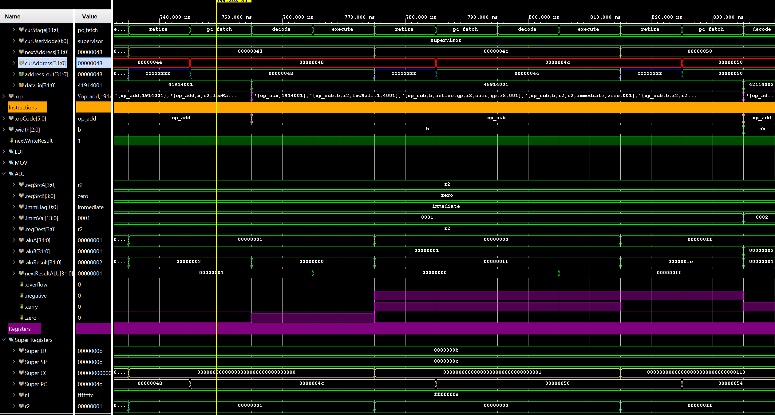
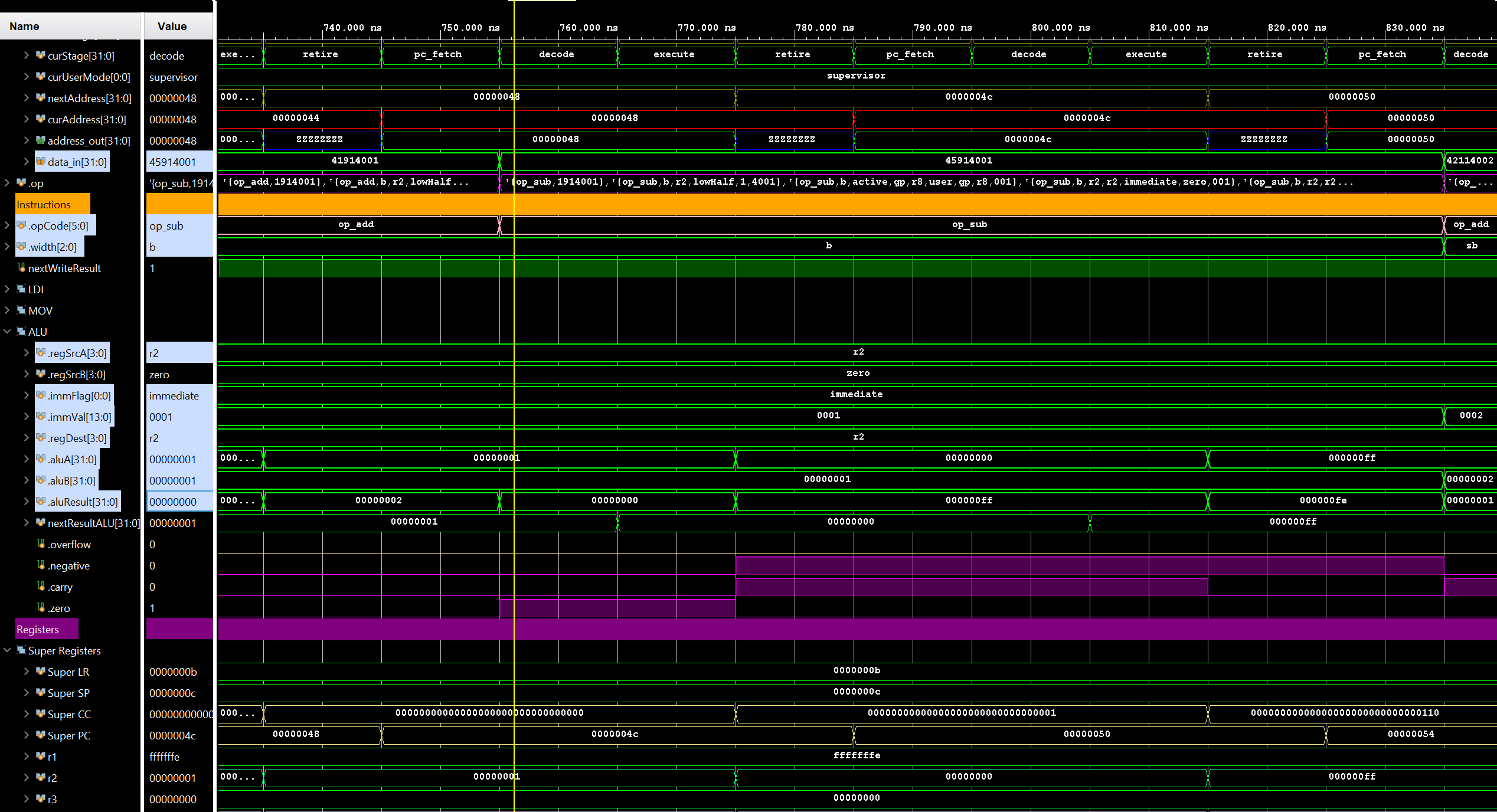
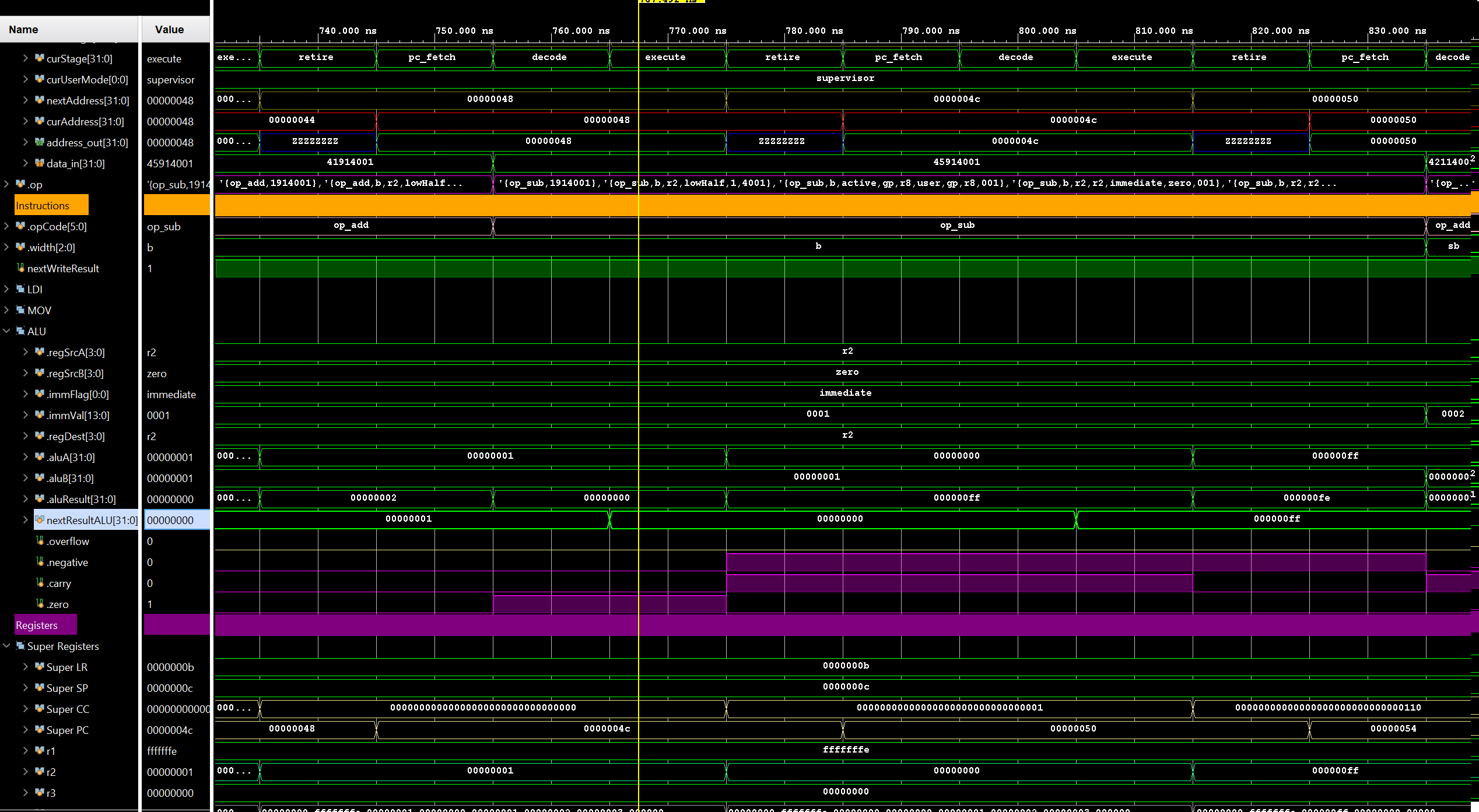
Integrating Ember into an LLVM backend was considerably more complicated than I imagined, based on what little documentation and information I managed to find on the web. What I thought would take a few weekends, ended up taking many weeks of hacking, with my day job and other distractions. However, I did manage to get it working and output Ember32 Elf files. 

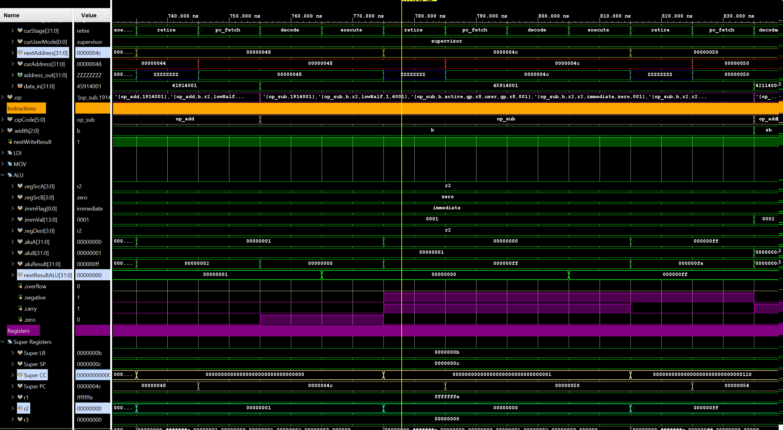
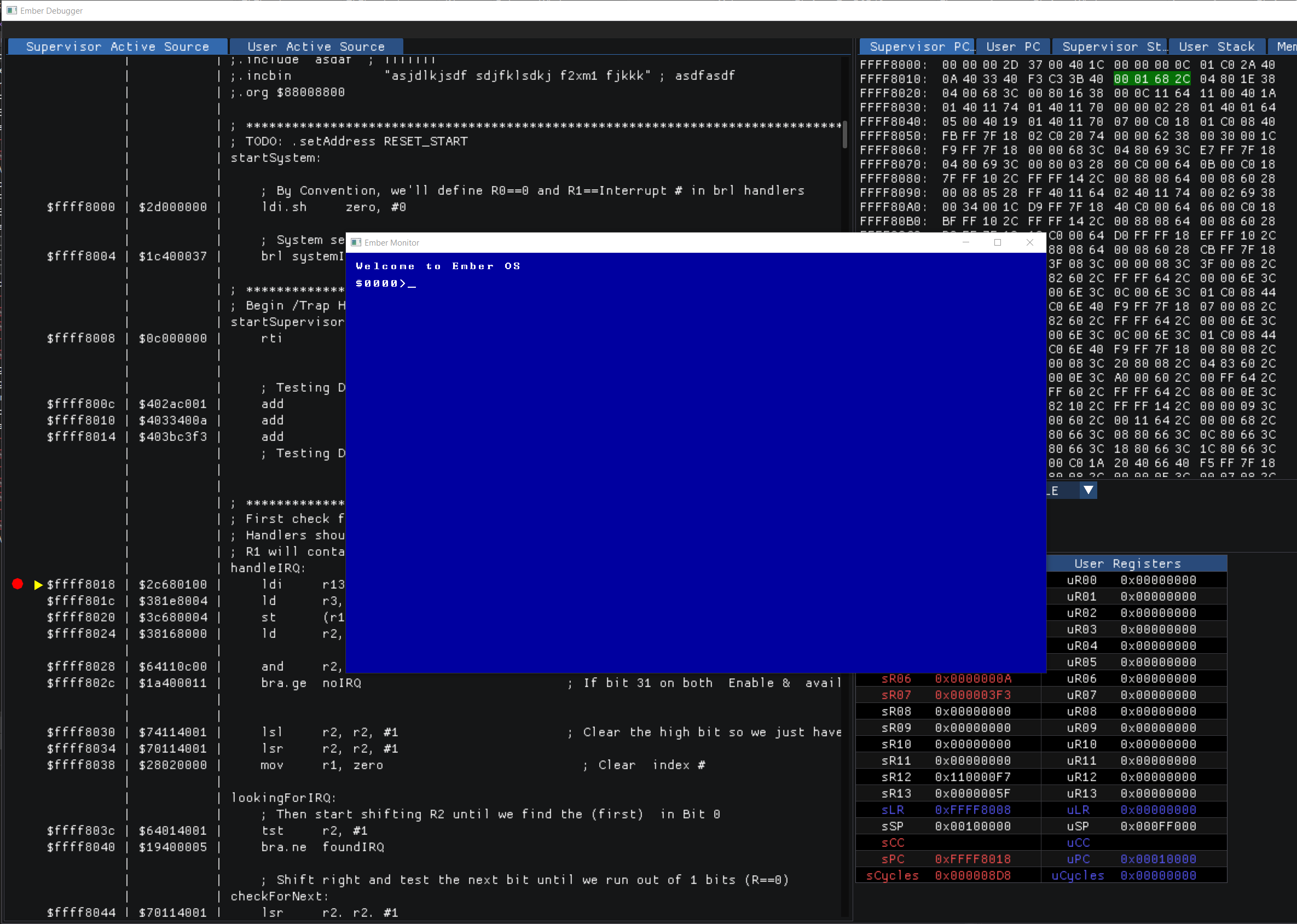
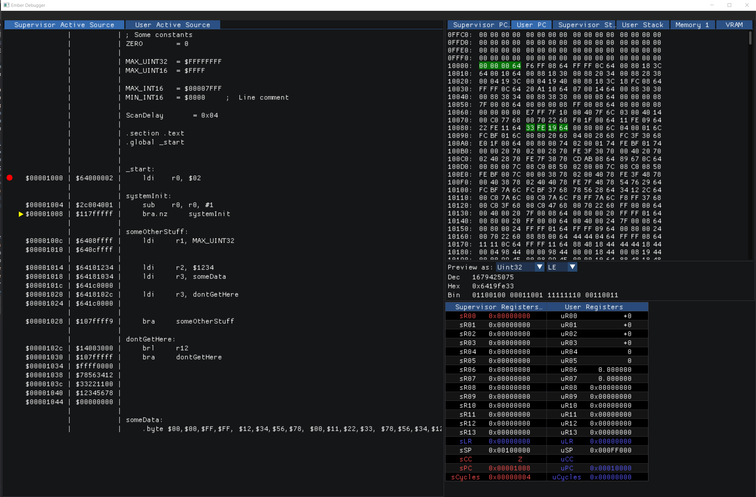
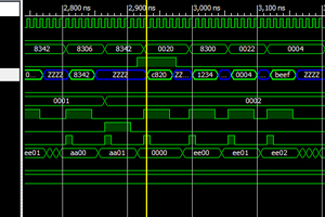
The next step was to implement an ELF loader in the emulator, and also support for DWARF debugging info in the ELF. So now I can load and run LLVM-generated ELF executables in the Ember emulator, and use the runtime debugger to step through the source running on...

Read more »

  • Project Update

    Tom10/30/2022 at 15:24 0 comments

    Just a heads up, this project is still moving forward, slowly, my computer game consulting company IARItech.com has been busier than ever, taking up nearly all my time, along with the search for a new boat. That said, I have been making some progress, mostly on the emulator and debugger.

    Ember Debugger
    Ember Debugger Window

    I started working on a basic system monitor in Ember assembly, while also improving the assembler and debugger functionality as I go, then I got caught up with separating the integrated emulator and debugger into separate applications. Previously they were the same app, with the debugger being the emulator, and a separate window showing the output of the virtual machine.

    Ember Emulator Window
    Ember Emulator Window - Testing printf implementation

    I have now separated the two and I’m working on a socket-based network debugging protocol. The advantage will be that the emulator can run on a separate machine from the debugger. There are two scenarios that come into play here, one is running the emulator on a Steam Deck or other portable system, and the other is debugging Ember code directly on FPGA hardware, we’ll need a debugger that can connect to an FPGA fabric debugging harness, or possibly a debugger/monitor running as system software on the actual hardware. 

  • Uploading llvm-mc elf to FPGA and Simulation

    Tom02/18/2022 at 20:20 2 comments

    After a lot of pain and suffering(tm), I managed to get Vivado to update the bitstream to contain the contents of an Ember elf binary! 

    I honestly had no idea how convoluted integrating the assembler would be, but it appears to be working now, and each time I implement the design, the tool automatically adds the binary data to the BRAM initialization block so the program is on the FPGA when it starts. To get this working, I created a tcl script to update a mem file containing the binary data for simulation and implementation, and another to just patch the bit file if I'm just updating the assembly program (so I can just upload the patched bit file, not wait minutes for a new one to be implemented...)

    Previously, I just built the instructions using {, , , } syntax in the memory definition, which is not a solution long term. It required a full re-synth/impl pass just the change a bit in the test program, and also, writing instructions required hand-constructing the opcodes. Now I can just write normal assembly in an editor, assemble it with llvm-mc, link it with llvm/lld, then run the scripts to patch the resulting elf file.

    Previous method (in .sv file for BRAM module):

    30'h00000000: data.mov <= '{OpCode::op_mov, WidthCode::w, MovReg::active, RegSet::gp, Reg::zero, MovReg::active, RegSet::gp, Reg::r2, 11'h000 };
    30'h00000001: data.mov <= '{OpCode::op_mov, WidthCode::w, MovReg::active, RegSet::gp, Reg::r2, MovReg::user, RegSet::gp, Reg::r3, 11'h000 };
    30'h00000002: data.mov <= '{OpCode::op_mov, WidthCode::w, MovReg::active, RegSet::system, SysReg::pc, MovReg::user, RegSet::gp, Reg::r4, 11'h000 };
    30'h00000003: data.sys <= '{OpCode::op_halt, 26'h0 };
                        
    30'h00000004: data.mov <= '{OpCode::op_mov, WidthCode::h,  MovReg::active, RegSet::gp, Reg::r2, MovReg::active, RegSet::gp, Reg::r1, 11'h000 };
    30'h00000005: data.mov <= '{OpCode::op_mov, WidthCode::sh, MovReg::active, RegSet::gp, Reg::r2, MovReg::active, RegSet::gp, Reg::r1, 11'h000 };
    30'h00000006: data.mov <= '{OpCode::op_mov, WidthCode::b,  MovReg::active, RegSet::gp, Reg::r2, MovReg::active, RegSet::gp, Reg::r1, 11'h000 };
    30'h00000007: data.mov <= '{OpCode::op_mov, WidthCode::sb, MovReg::active, RegSet::gp, Reg::r2, MovReg::active, RegSet::gp, Reg::r1, 11'h000 };
    

    Assembly file version:

    .org 0
    _start:
    
        // MOV Test
        mov      zero, r2 ; write nothing
        mov      r2, ur3  ; user r3 to r2
        mov      pc, ur4  ; skip the following halt
        halt
    
        mov.h    r2, r1   ; 16-bit (zero extended) r1 to r2
        mov.sh   r2, r1   ; 16-bit (sign extended) r1 to r2
        mov.b    r2, r1   ; 8-bit (zero extended) r1 to r2
        mov.sb   r2, r1   ; 8-bit (sign extended) r1 to r2
    
        ...

    Making this work requires the use of the Vivado updatemem.exe tool (which replaces the data2mem.exe tool since about 2015 or so). It is not as simple to use, but once it works, it is quite useful. 

    Unfortunately, there is not a lot online about the newer tool (outside of the intended use with their MicroBlaze IP), but I managed to piece it together, mostly by looking at .mmi and .smi files people have made and posted online for their CPUs, which mostly use AXI busses also. If you are not using a Xilinx IP, or a core with AXI, you can't use their integrated ELF support, unfortunately. This site was particularly helpful if you are interested in the details of creating a .mmi file.

    MMI and SMI Files

    To use updatemem.exe, I first had to create a .mmi file, which describes where the BRAM is located on the FPGA, and how it is configured in the bitstream. Here is what I have for my very simple 4k test RAM (basically 1 32(+4p)-bit BRAM block on the Spartan7):

    <MemInfo Version="1" Minor="5">
      <Processor Endianness="Little" InstPath="my_bram">
        <AddressSpace Name="my_local_bram" Begin="0" End="4095">
          <BusBlock>
            <BitLane MemType="RAMB36" Placement="X0Y3">
              <DataWidth MSB="31" LSB="0"/>
              <AddressRange Begin="0" End="1023"/>
              <Parity ON="false" NumBits="0"/>
            </BitLane>
          </BusBlock>
        </AddressSpace>
      </Processor>
      <Config>
        <Option Name="Part"...
    Read more »

  • ALU, LDI, NOP, HALT at 100MHz - Part 2

    Tom02/08/2022 at 18:45 0 comments

    I previously walked through and LDI instruction, this time we will look at how the stages of an Ember ALU instruction operate...from a high level at least. This implementation, while far from finished, does run at 100MHz currently, however, looking at the timing analysis in Vivado, some of the paths are getting quite close to the 10ns limit between clock cycles.  The Z and N flag operations are the last to complete, since they rely on the result of the ALU op, so I'll have to take a look at those to see if I can change the logic around to get better inference.

    For now, let's look at the SUB instruction in the simulation timeline view.

    As with any instruction, the first thing that happens in the pc_fetch stage is that curAddress (and thus address_out) is updated with the value of nextAddress, which was set in the retire stage of the previous instruction. In this case, the address to fetch is 0x00000048.

    In the decode stage, we see that a sub.b instruction has been fetched by looking at the op.opCode and op.width values. Because of the b modifier, the width of the operation is 8-bit unsigned (zero-extended) byte. This means that both the input values and output of this instruction will be masked and then zero-extended. In addition, the processor ALU flags will be set based on the value of the 8-bit result.

    If we examine the rest of the decoded instruction, we see that op.regSrcA is register r2, which currently has the value of 0x00000001. Also, op.immFlag is set, so the immediate value 0x01 contained in op.immVal is used for the second operand. This describes the following instruction in mnemonic format:

    sub.b r2, r2, #1

    The equivalent C would be:

    uint32_t r2 = 1;
    r2 = (uint32_t)((uint8_t)r2 - (uint8_t)0x01);

    In the execute stage of an ALU instruction, the CPU will latch the result registers to the values in the output. These include aluResult, which now has the value 0x00000000, as well as the ALU flags overflow, negative, and carry, which are all unset except zero, which is set since the output value is 0.

    You might also note that after the execute stage, the address_out bus is released (represented by ZZZZZZZZ, or high impedance), since the value is data_in is no longer needed. In a real system, this would disable the memory read line on the CPU to allow other devices on the system bus to access memory if needed.

    Finally, the retire stage is where the values of the flags and aluResult are written to the CPU registers, and we also update the nextAddress again to point to the next instruction.

    Also notice that a bunch of values in the timeline change at this point, like the flags and operands, but we don't care since these only matter at the time they are latched into registers. Since they are always wired to the data_in register no matter what value is there, they become basically undefined when the address is not being driven by the CPU directly.

    That covers the ALU instruction from the timeline view. I'm working hard on an ISA document, which I will post soon, and should make much of this more clear, and open for discussion. 

  • ALU, LDI, NOP, HALT at 100MHz - Part 1

    Tom02/07/2022 at 01:37 0 comments

    Success! The FPGA implementation can execute at least a few of the instructions at 100MHz on the Spartan Edge! Keeping in mind it's a simple test, running about 34 instructions: first, a bunch of LDI (Load Immediate) instructions load registers, then a combination of ALU instructions perform a sequence of ADD, SUB, etc. at various widths 8-bit, 16-bit, and 32-bit operations on registers, then NOP and a HALT, ending with the correct final results and flags. I can also step through the entire sequence of instructions one cycle at a time and watch the CPU stages, flags, and one register (r2) on the LEDs.

    Here you see the final stage after running the test program. On the left 0b101 (stage 5 == HALT), then 0b010 (CPU Flags Carry/Negative/Zero so N flag set), and in red the low 8 bits of register r2 0b11111110 (-2 signed).

    To see how I got here, we can look at the Logic Analyzer time view in Vivado. First, a few quick notes: 

    Currently, all implemented instructions take exactly 4 cycles, represented by the following Stages:

    • pc_fetch - Request the next instruction from memory by promoting the value of the internal register nextAddress (which was set in the previous retire or reset stage) to curAddress, then assigning the memory bus address_out to that value for at least a cycle to load the instruction word
    • decode - Load the new instruction word from the data bus data_in into the internal op register. All the appropriate connections to the ALU and other instructions are always wired, so they decode the result "immediately", available after only gate propagation delay in the same clock cycle.
    • execute - Results of any operation (and appropriate flags and CPU states) are latched in internal registers. This is necessary especially in cases where one of the source registers is also the destination register location.
    • retire - Write out latched results to the destination register, set processor flags, set nextAddress for the next pc_fetch.

    There are also two others:

    • reset - In this state while sys_rst is high
    • halt - After executing a HALT instruction, stays in this state until sys_rst goes high. Useful for debugging/testing.

    There are currently no wait/stall stages, as there are no memory or branch instructions so far, and I'm using Block RAM right now which always completes in 1 cycle, so we don't need to wait on a signal to read or write the memory value. Ultimately I will need to add these.

    Ember Vivado Timeline - Retire

    Now that you know what should be happening, let's look at it in the timeline. We will actually start on the last stage of the previous instruction indicated by the verticle line. Notice that nextAddress is incremented here to 0x00000004. If the previous instruction were a branch, it might have instead set the address to the branch target location at this point.

    Ember Vivado Timeline - pc_fetch

    We now start the next instruction with the pc_fetch stage. Notice that the register curAddress is updated with the value of nextAddress, and address_out is wired to curAddress and the address 0x00000004 is sent out to BRAM.

    Ember Vivado Timeline - Decode

    One cycle later we are in the decode stage. Here we see that data_in now has the instruction word available, which is latched into the op register. This register is cleverly defined as a union of structs, each describing one type of instruction. These structs are in turn continuously wired to their respective logic so that when the 32-bit value is loaded into the register at the start of the decode stage, the results are computed for all possible instructions simultaneously in parallel in hardware. Only after we examine the opcode in the later cycles do we choose from the various results and write out only the information we need.

    In this case, we have loaded an LDI instruction designated by op_ldi in the opCode field, so we can examine the LDI struct to see the contents of the instruction word. One bit labeled hiloFlag here determines if the 16-bit Immediate value immVal goes into the...

    Read more »

  • Progress on the ALU FPGA Design

    Tom01/28/2022 at 02:17 0 comments

    I have made some great progress on the ALU in SystemVerilog in Vivado for the Spartan-7. I can now step through a sequence of ALU instructions, have them read from registers and immediate values, then save out the result to another register. The next step will be to add some additional instruction types to the decoder logic, probably memory load/store, and a few others like load immediate to have some data to operate on. Then I need to try stepping it on the FPGA hardware. For now, it is looking good in the simulator.

    Vivado Simulator View of Ember ALU

    I decided to go with SystemVerilog ultimately. Originally, I wanted to do the whole implementation in Verilog, but after finding roadblocks and bottlenecks (a lot of it was due to being a programmer for decades, Verilog was just too limiting), it was becoming apparent it would be much harder to do.

    Anyway, as you can see from the simulator image above, there are benefits to using SystemVerilog and going all in. I was able to define typedef enums for all my types and values. Then I defined a number of structures for each encoded instruction word, defining the bits in each instruction and assigning them enums. This way, I can just load the 32-bit instruction and set it to a typedef logic union, then use the structure members just like it was C code! It looks like it's just as optimal, way easier to read, and even more convenient to simulate.

    If you look closely at the sequence in the image, you can see all the values with names like the pipeline state at the top, names of instruction opcodes, registers by name, etc. I can then change their colors as well. People complain all the time about the "closed" tools like Vivado, Quantus, and the like, but so far it has been working for me...we'll see as I get farther into things. I have to say it is slow when building for hardware though...you do need a fast machine or builds take forever...

    I plan to write up something on the SV code at some point, but right now I'm having so much fun just coding it! :)

  • FPGA Test Harness

    Tom01/23/2022 at 21:16 0 comments

    In preparation for ALU development on the FPGA, I decided to hook up all the external pins of the Spartan Edge board to LEDs and switches so I can do at least a bit of debugging. Ultimately, once I have more of a working CPU, I can likely interact through the ESP32, I2C, or something. But for now, it will be more hands-on. First, though, I had to solder on the headers for various connections (using my brand new digital microscope!), as the Spartan Edge leaves those off initially as verious user options to install as needed.

    Soldering the Spartan Edge

    The Spartan Edge board has various connections to the Spartan-7 FPGA and the ESP32 onboard. Many of the IO pins from the Spartan-7 are laid out and configured with resistors to be used with an Arduino Uno, and a few are directly wired. We have 14 pins from the Arduino Digital IO headers, and 10 pins from the FPGA directly. Unfortunately, the Analog pins are instead wired directly to the ESP32, which is all fine, but since we're not using that right now it isn't helpful. 

    One very unhelpful note is that there are NO 3.3v pins at all (at least on any of these headers) to get VCC_3v3 from the board! I did some checking, and the ONLY place you can get regulated VCC_3v3 from the board is the two Grove connectors, which are intended to be used for I2C or whatever, and the JTAG connector which I need in order to program the FPGA. I didn't have any Grove connectors, so I'll need to wait for them to come in later this week. Unfortunately, the pins are too small to get female jumper wires to stay put.

    First Pass Debug Connector for Spartan Edge

    For now, I can at least set up the breadboard with some LEDs and switches. My first attempt was to just place the board directly on two short breadboards, which would be way cleaner, however, I soon realized that all the pins I need are on one side of the board, and if I run jumper wires to the breadboard, I can't use the top row of connections if the board pins are connected. So, on to plan B...

    Now I have the FPGA board plugged into the breadboard, mostly just to hold it in place, as I am not currently using any of the analog or signal pins from that bottom Arduino header. I then run ribbons of IO pins to the breadboard. Initially, I'm running the Arduino 0-13 pins as output driving the LEDs in sets of 8, 4, and 2, and the 10 FPGA pins to switches in 8 and 2. Here they are just tied to Ground, since I don't have the VCC side wired yet, so the switched inputs float when not grounded...resulting in noise, but I can at least see they are working.

    There are also some switches, two pushbuttons, and a few LEDs on the board if I need those. I figure I can use the pushbuttons to step through test cases.

    Next up, get some ALU functionality coded up on the FPGA so I can step through some logic on the test connections.

  • HDMI "Mode 0" Text Output functional on the Spartan Edge FPGA

    Tom01/16/2022 at 18:58 0 comments

    While I have been working on the emulator and assembler, I have also been playing around with the Seeed Spartan Edge FPGA. After watching an untold number of videos on You Tube, and reading through a few (unfortunately too few) GitHub projects, I have managed to implement an HDMI output example in Verilog for the Spartan 7 FPGA.

    Spartan Edge FPGA

    It currently only supports a single resolution at a time, set to 1280x720 for now. I have tentatively called "Mode 0" (the only one at this point really) as an 80x45 character text mode using a 16x16 bit ASCII font. For this test case, I store both the default VRAM contents (80x45 bytes) and the font (128x2x16...half the ASCII character set, plus 2 by 16 bytes for each character bitmap) in block RAM on the FPGA.

    FPGA HDMI Output
    The next step for the FPGA project is to create some code to write data to the dual-port block RAM, so the HDMI output can display text. I figure the first step for that is to work on the ALU and CPU pipeline implementation. That will at least allow some part of reading and writing to memory.


  • Display Output and Keyboard Interrupts Working in Emulator

    Tom01/15/2022 at 20:20 0 comments

    I now have the emulator back to the point I was before I started integrating the LLVM assembler and linker! This means when the emulator is running it outputs to a virtual 1280x720 text display (80x45 16x16 characters for now) with a very simple monitor program that can read keyboard input. The display and keyboard controller work through CPU interrupts.

    I will go into detail on how this works once I get my Medium Blog caught up. I'm still going through early design at this point at a very high level, but I will get way more detailed soon.

  • Quick Progress Update

    Tom01/10/2022 at 18:00 0 comments

    Been a while, thought I should just give a heads up. I have the emulator and LLVM assembler working now with nearly all the instructions, including branch and memory access. The debugger now supports stepping and breakpoints for supervisor-level code (think kernel/firmware)...need to add support now for user-level code (applications), then I can hook up the rendering and keyboard interrupts again (broken since the change from my hacky assembler days to LLVM)

    I have also been making progress with the FPGA. I worked over the weekend to get a simple Mode0 HDMI output working. I can now at least fill the screen with the letter 'A'! I know, sounds like not much, but for me it's a milestone. I now need to get the Block RAM VRAM working, issues with clock timing I need to work out...then I can output text on the HDMI screen attached to the FPGA. Next step will be to start coding the ALU for the CPU.

    Cheers, Tom

  • Emulator/Debugger now working with LLVM-produced *.elf files

    Tom12/23/2021 at 22:40 0 comments

    With a few days off for the holidays, I finally had some time to get the debugger working again. It now supports the common DWARF debugging standard segment that is contained in the ELF file written by LLVM-MC and LLD.

    I originally coded it for the simple assembler that I wrote for the CPU, but the system quickly outgrew that and I decided to implement a "real" assembler. I ended up going with LLVM-MC over a separate assembler like VASM so I could more easily implement higher-level languages at some point. That was painfully complex, but it is now working, at least for a small subset of the Ember instruction set.

    I can now set breakpoints, step through the code in the emulator, as well as view and edit registers and memory, directly in the emulator window. 

    Next, I need to finish up the instruction set ISA, add all the remaining instructions to the LLVM TableGen scripts, then update the emulator for the new instructions and I should be able to get working on some firmware/OS code. 

View all 13 project logs

Enjoy this project?

Share

Discussions

Similar Projects

Does this project spark your interest?

Become a member to follow this project and never miss any updates