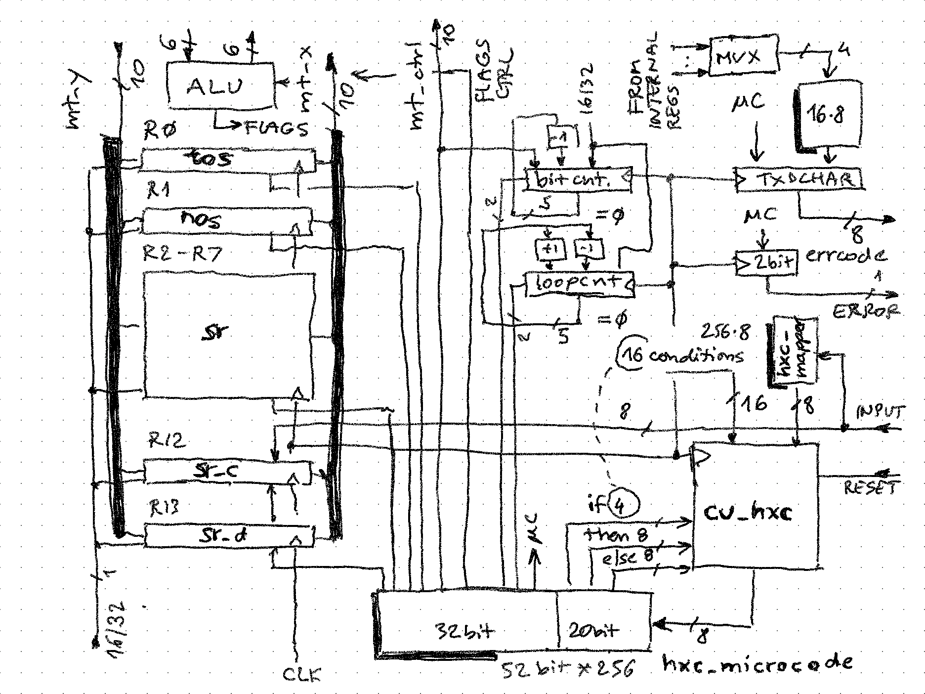
Close
0%
0%

Bit-serial CPU based on crossbar switch

256 switches and few shift registers to implement a working 16 or 32-bit integer arithmetic calculator (+, -, *, /, isqrt, BCD / bin conv..)

Public Chat
Similar projects worth following
Bit-serial CPUs were not a rarity in early days of computing, and especially not for calculators in the discrete or SSI/MSI era (before mid-70ies). Their biggest problem was of course speed.

But what if more than 1 bit-serial operation could be done simultaneously? If the number of simultaneous serial operations approaches the length of processing word, then the serial CPU could come close to speed to a parallel computer with same word length!

In this project the parallelization is achieved using a matrix of cross-bar switches that can connect any and all shift registers to any and all 1-bit processing units.

To move from theory to practice, a stack-based integer calculator is implemented to illustrate the concept. The implementation is done partially in hardware (2 MT8816 cross-bar switch ICs on breadboard) and partially in software (microcode-driven custom processor).


CPU architecture

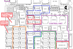
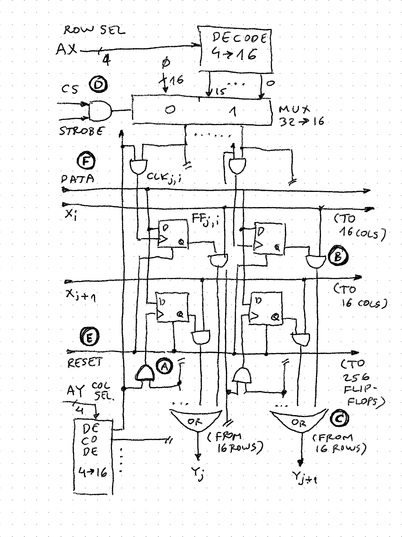
A simplified schematic of the CPU illustrates the main components:

  1. The switch matrix - the inputs (rows) are connected to the outputs of registers and outputs of processing elements, while outputs are inputs to registers and processing elements. Any number of switches can be on or off, and this is done under program control (microcode, or state machine). It is important to note that output column wires have "pull-down" - this means if no switch is on in that column, the output will be 0. This way, logical OR can be implemented on any number of inputs simply turning on multiple switches in a column (of course, an opposite implementation could generate a wired AND)
  2. Register stack. In simplest form, they are shift registers with common clock - at each clock time 1 bit is presented to their outputs (going into switch matrix) and 1 bit picked up on opposite side (from switch matrix). If the word length is n bits, after n cycles the value in register is unchanged. 
  3. ALU operators. These are either simple logical gates (NOT, NAND, XOR etc. - note OR is not needed as it is "baked into design") or 1-bit state "machines". For example a full-adder requires a 1 bit carry flip-flop to keep the carry between each bits as they are added, or a delay flip-flop that allows implementing shift up/down operations. Both of these flip-flops can be set/reset/unchanged under program control, and their state examined for branching etc. 

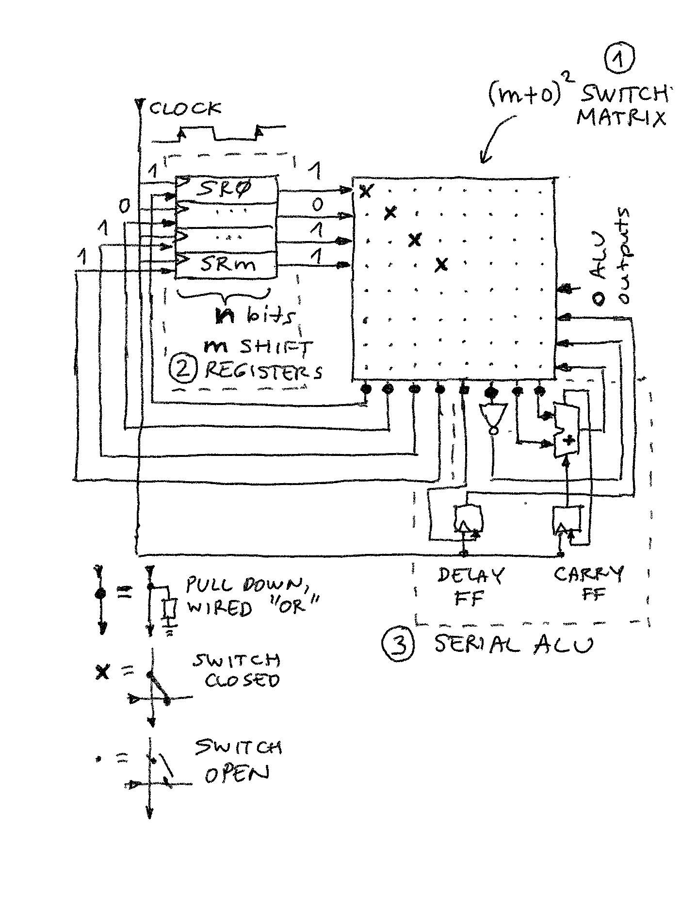
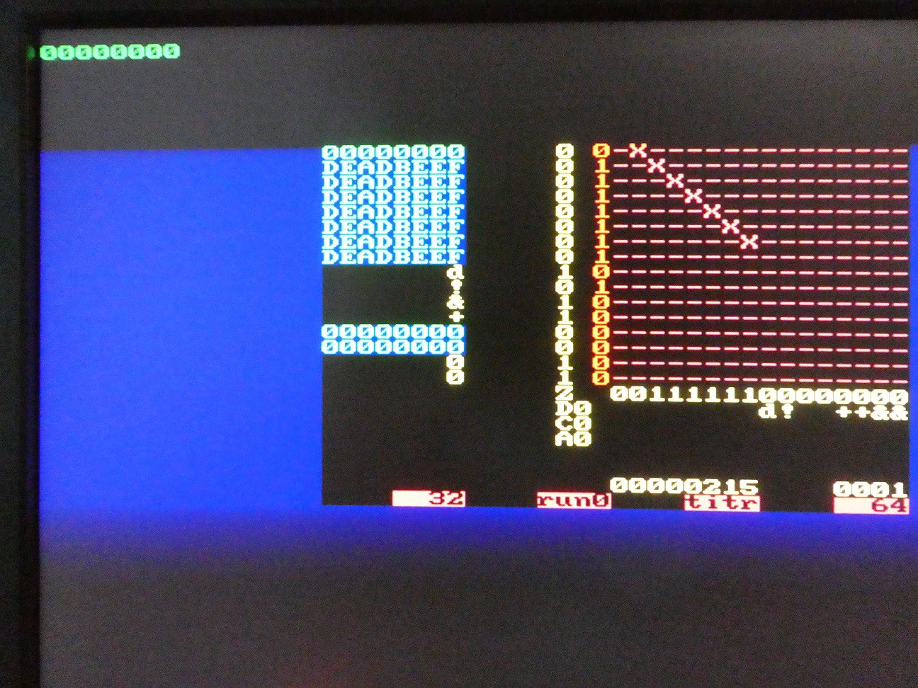
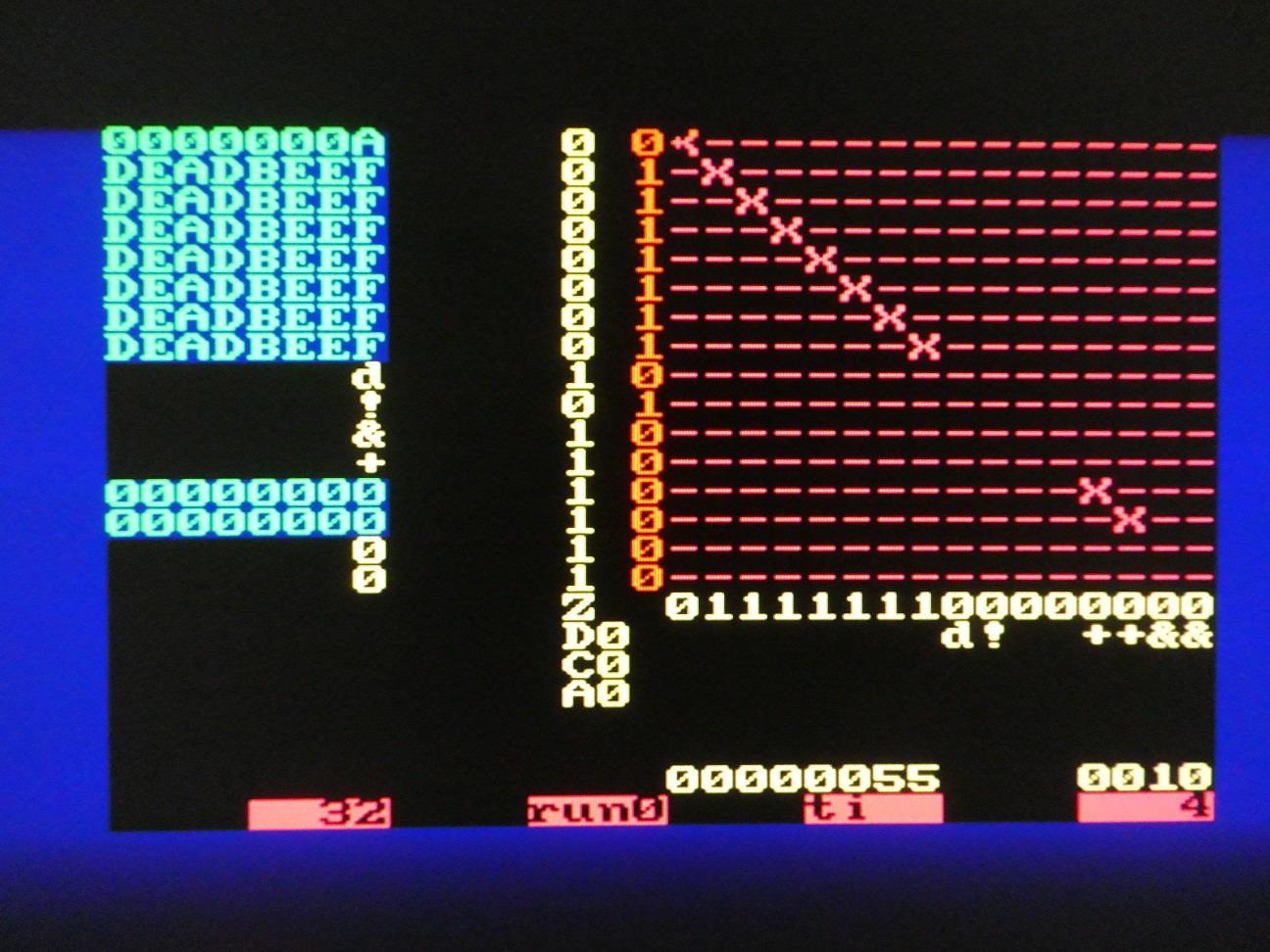
NOP operation is illustrated - all switches are OFF except the ones on the "register diagonal" - this means the "head" of each register is connected to its "tail" so after every n clock cycles nothing changes. 

Move and logical operations

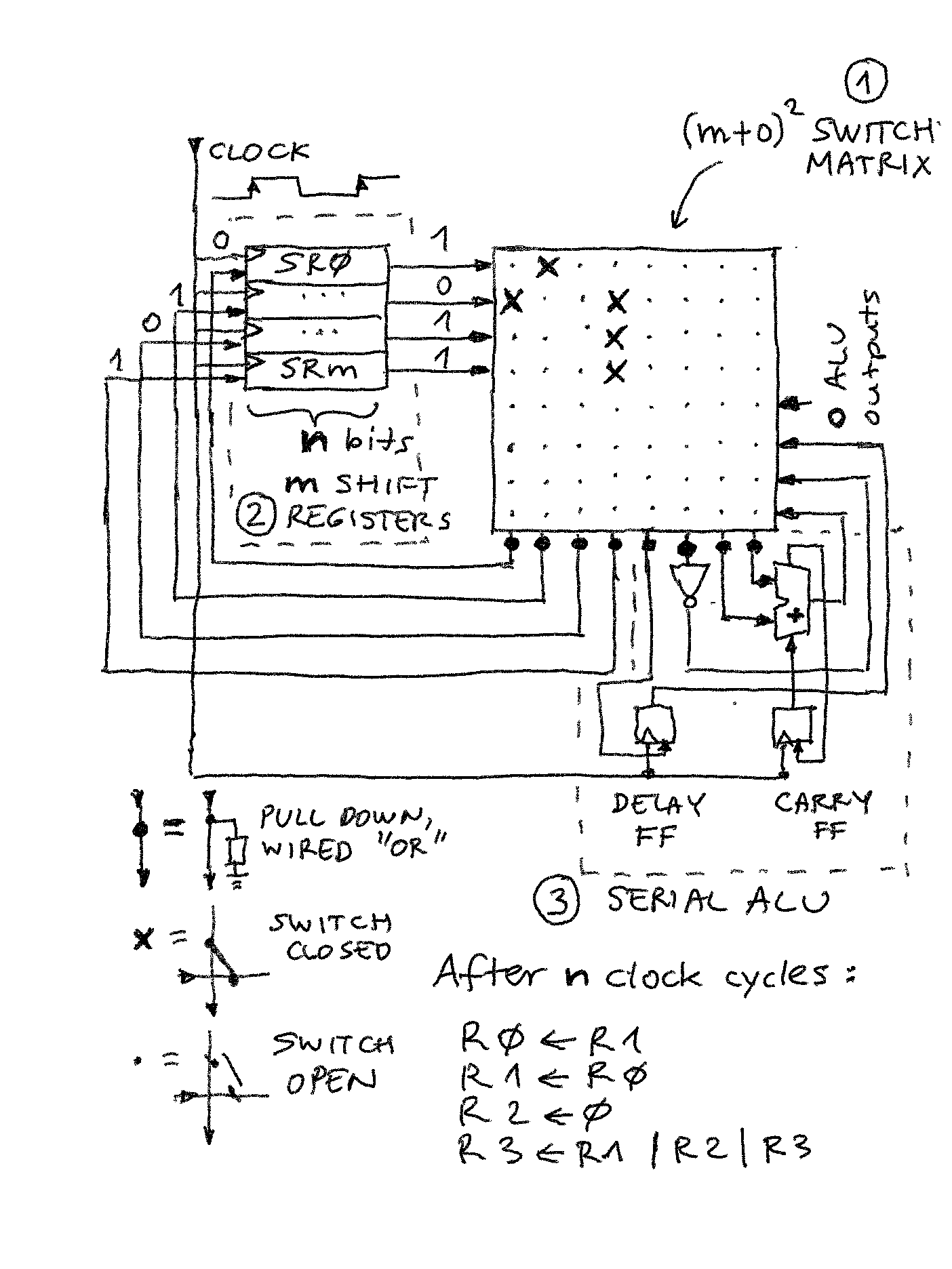
With switches on only in the "register quarter" top-left, many moves, loads, and logical operations are possible. It is best to read by columns:

  • 0: connected to row 1, therefore R0 <= R1
  • 1: connected to row 0, therefore R1 <= R0
  • 2: not connected, pull-down will keep it at 0, so R2 <= 0
  • 3: connected to multiple rows, 1 on each of them will pull the column up to 1 (wired OR), R3 <= R1 | R2 | R3

Note:

  • 4 operations can be executed in n clock cycles
  • exchanging registers possible without temp storage
  • number of inputs and outputs is flexible (for example result of R1 | R2 | R3 could have been assigned to all 4 regs at once!) unlike standard 1, 2, 3 operation field instructions of most CPUs.

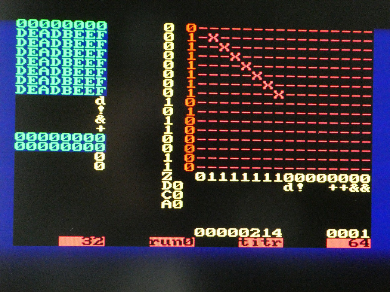
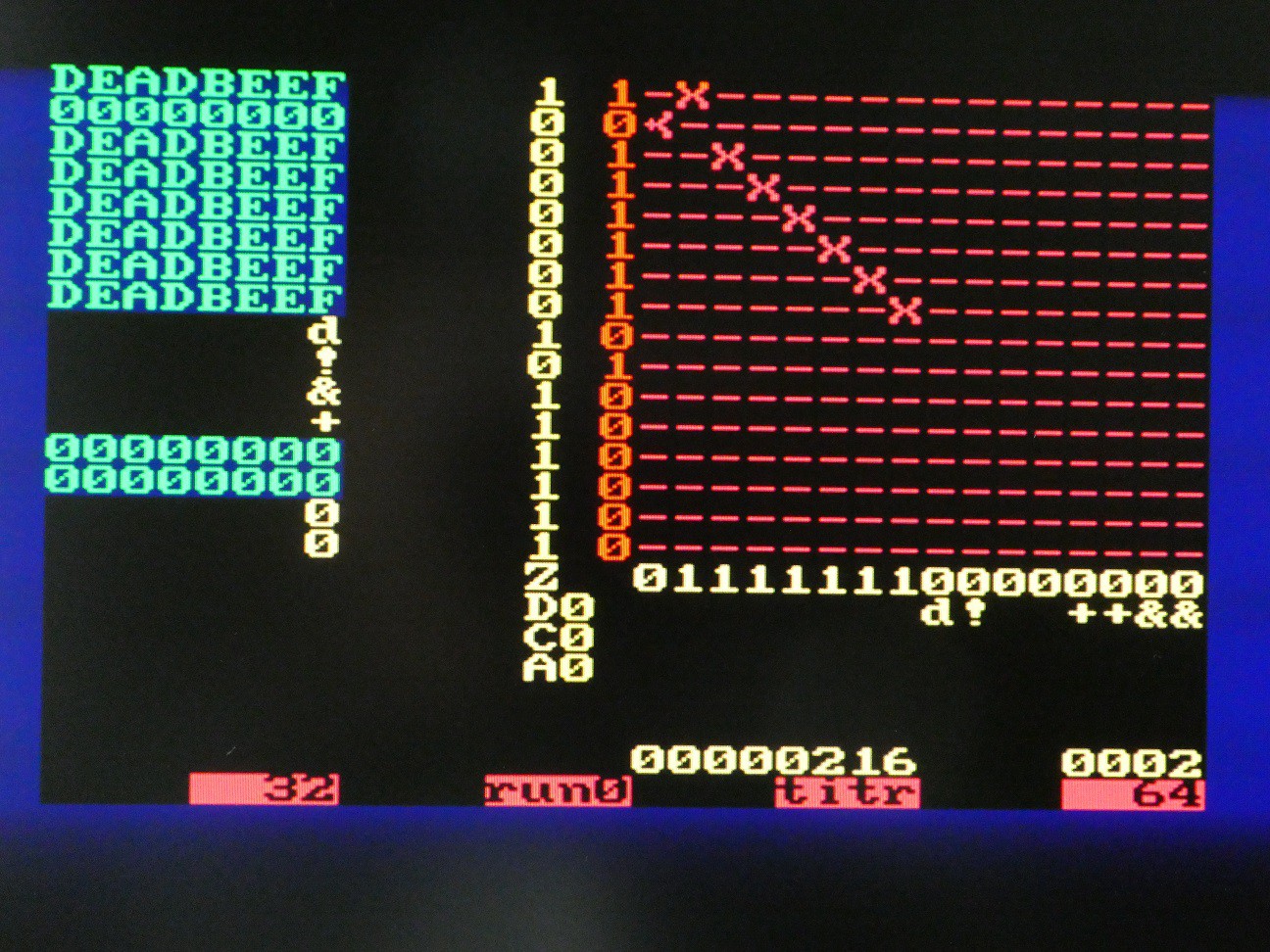
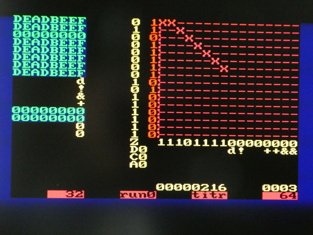
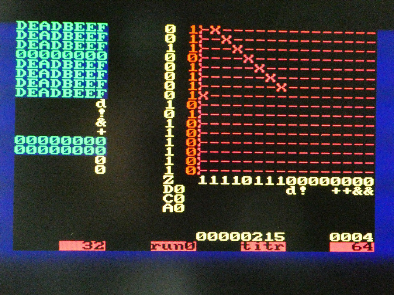
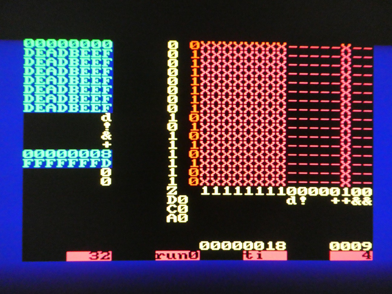
Arithmetic and logic operations 

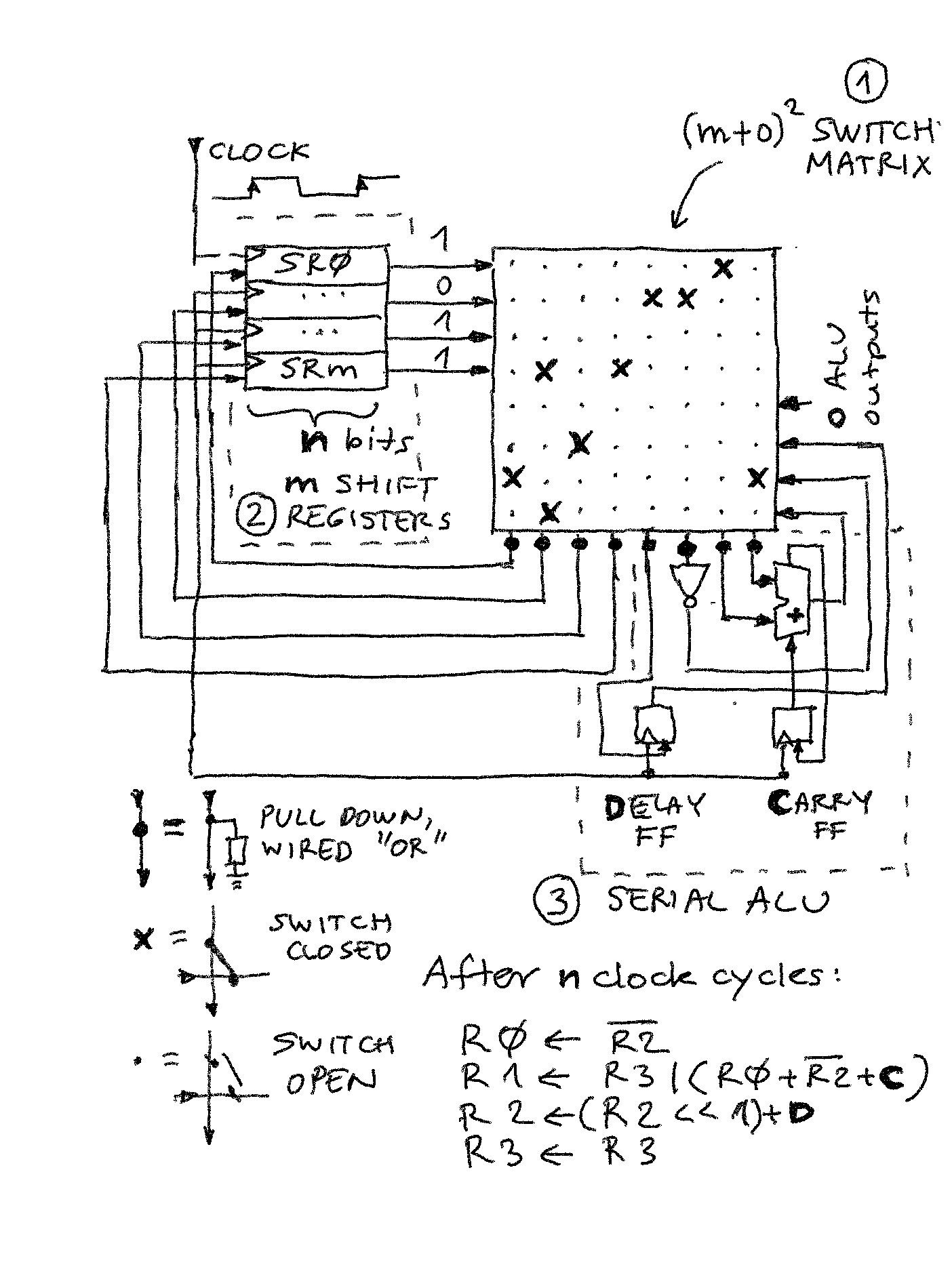
The connection matrix is more complex now. Register assignments are read column-wise 0 to 3:

  • R0 is output of NOT
  • R1 is OR between R3 and output of full adder
  • R2 is output of delay flip-flop, so will be what went in there in cycle n-1
  • R3 is connected to itself only (NOP)

The connections to ALU elements are read by columns 4 to 7:

  • delay flip-flop input is R2
  • NOT input is R2
  • first input of adder is R0
  • second input of adder is output of NOT

Combining these, we see the results of register updates on the pic. If the shift direction is LSB first, and C is set to 1 initially, R0 - R2 is executed. Of course, the result does not need be stored so a comparison operation can be executed along with copy, set etc. 

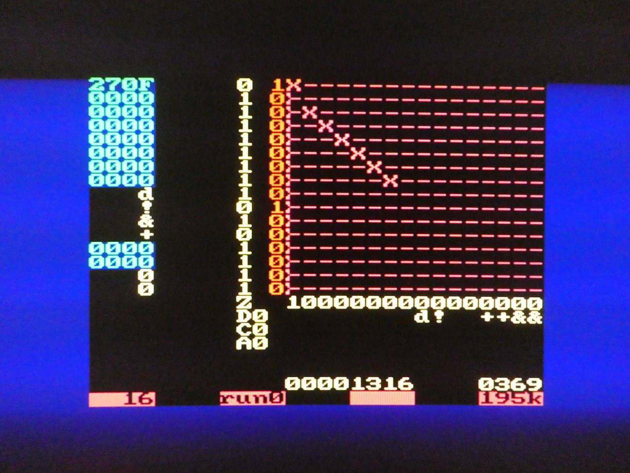
Delay bit processing

Delay bit can be used to implement any number of shift and rotate operations. If R contains r7...r0, then:

  • LSB shift after n cycles: r6 r5 r4 r3 r2 r1 r0 D ("logical shift left")
  • MSB shift after n cycles: D r7 r6 r5 r4 r3 r2 r1 ("arithmetic shift right" if D is set to r7 initially, or "logical shift right" if set to 0 initially)
  • Matrix can of course be reconfigured during the shift to inject D at any point so it can appear anywhere in the final register value 

sys_sbc8816.bit

Ready to be uploaded to Anvyl FPGA board. isqrt(1) correctly returns 1, no error.

bit - 1.42 MB - 04/26/2022 at 04:20

Download

  • Running serial CPU at 25MHz!

    zpekic09/06/2022 at 04:40 0 comments

    As noted in other logs, it was difficult to run the CPU at >2MHz or so, most likely due to R/L/C impedances and skewed signals from 6+ in wires from the PMODs to breadboard holding the 2 physical MT8816 ICs.

    But what if the switch matrix was inside the FPGA, not outside, how fast could it run? To try that out, I developed a "virtual replacement" for the 16*16 switch matrix, and called it (very original!) MT16x16

    Replacing a true analog switch array with FPGA would be only possible using very fancy and expensive FPGA chips which have analog paths. Luckily, MT8816 in this design is used as a "wired or" not really analog, so it is possible to create 256 D-type flip-flops, each controlling an AND gate connected to a row input (X), and 16 of these OR'd together make up a column output (Y):

    Noted on the schema above:

    • (A) - the clock for each flip-flop is generated by 2 input AND that registers the coincidence of row and column selection. This way only at most 1 FF can take the DATA input  (same as real MT8816)
    • (B) - FF output (traditionally marked Q like in classic 7474) is used as an "enable" signal to AND with the input row X
    • (C) - 16 outputs of AND gates (B) are then OR'd together to form output column Y. The "wired OR" becomes clear - if at least 1 FF in the column is "set" and its X input line is high, the output of column will be high. 
    • (D) - while column decode (AY) is always active, row decode is only active when CS (chip select) and STROBE signals are both high. Outside component drives these signals from microcode, but enables them only during 4-phase clock phase 1 (to insure right signal levels are propagated before clocking the FFs)
    • (E) - reset signal is routed to 265 FFs - this is very bad design in FPGAs are routing resources are limited, but it worked. Outside component also drives reset signal from microcode and phased clock to prevent misfiring (microcode only used 2 bits to encode set, clear, reset all and nop - in hindsight this was a bad design decision because probably with 1 hot encoding (and just 2 bits more wide microcode word) the 4-phase clock would not be necessary.
    • (F) - data input is also routed to all 256 FFs

    In VHDL code, this 16*16 matrix is generated and interconnected using 2 generate loops. The column Y OR is pulled out of inner loop to make sure all ANDs are parallel and not stacked serially.

    With external wires eliminated, CPU can be driven up to 25MHz clock frequency (microcode execution at 6.25MHz due to 4 phase clock). This means that an integer square root of 32-bit number takes typically 16305 to 94195 cycles which means 2.6 to 15ms.

    CPU frequency is selected using switches 2..0 on the FPGA board. This gives 8 choices, the upper 4 of which select operation using internal matrix, and lower 4 with external (slower, but more fun!) MT8816 chips:

    -- select the clock
    with sw_clksel select mt_cnt <= 
        ss_cnt    when "000",    -- single step
        freq_2048(9 downto 8) when "001",    -- 4Hz        -- EXTERNAL MT8816
        freq_2048(5 downto 4) when "010",    -- 64Hz        -- EXTERNAL MT8816
        freq_50M(5 downto 4) when "011",    -- 1.5625MHz     -- EXTERNAL MT8816
        freq_50M(4 downto 3) when "100",    -- 3.125MHz    -- INTERNAL MT16x16
        freq_50M(3 downto 2) when "101",    -- 6.25MHz    -- INTERNAL MT16x16
        freq_50M(2 downto 1) when "110",    -- 12.5MHz    -- INTERNAL MT16x16
        freq_50M(1 downto 0) when others;    -- 25MHz     -- INTERNAL MT16x16

    Given that state of the matrix is reset and changed during the instruction execution (in other words, switch matrix state does not contain data to preserve from one operation to the next), it is possible to switch use of internal/external and back between instructions. Theoretically, it could be possible even to change the use while calculating an operation (because switch on/off commands are sent to both matrices regardless of which one is in use), but I haven't tried it and might fail due to glitches during such switch.

  • Operations: Q (integer square root)

    zpekic05/08/2022 at 02:36 0 comments

    With integer division, comparison, subtraction already implemented, it was possible to squeeze in integer square root as the algorithm can reuse these operations. Note:

    • all values in TOS are treated as positive (unsigned) integers, so it will never generate an error (root of negative numbers)
    • taking the root of full 32-bit numbers is possible
    • CPU has only 2 counters - bitcnt and loopcnt - the third "level of loop" does not use a counter in the CPU, but simply comparison with value executed in previous iteration

    The algorithm uses Heron's method described here. For implementation reference, see  to microcode lines 293 to 322 approx.

    1. First, argument in TOS ("S") is duplicated on the stack, dup() subroutine is used for this
    2. TOS is then shifted down (halved)
    3. If zero flag of TOS is set, we are trying isqrt(0) so bail with result 0 (but after 1 stack pop to not leave already duplicated argument in NOS)
    4. Note that 1 shifted down is also 0, which would give false result isqrt(1) = 0 - this is caught in div() subroutine by examining the delay status bit
    5. Now the stack is prepared to contain: X0, S, *, *, *, *, X0 - where X0 = S/2
    6. heron_step() is invoked to calculate the first iterative guess ("X1") which appears in TOS upon return
    7. root_loop: new "X1" and old "X0" iteration results are compared. This boils down to comparison between TOS and R7, which is a simple subtract with result not stored anywhere, just carry bit examined 
    8. if carry flag is set (X1 >= X0), iterations are over and result in R7 is copied to TOS, bail.
    9. root_cont: "new" X1 value becomes "old" X0 (which means R7 <= TOS)
    10. new X1 guess is obtained using heron_step() and proceed to step 7. 

    heron_step() subroutine implements the following calculation:

    x1 = ( x0 + s / x0 ) / 2;

    which is:

    TOS <= (NOS + DIV(NOS, R7)) >> 1

    // used as step in integer square root
    heron_step:    nuke, matrix_nop1();
            connect row_r7 to col_tos, div2(max, set);     // X0, S, S, ?, ?, ?, ?, X0
            divmod(same);                                // mod, div, S, ?, ?, ?, ?, X0
            nuke, matrix_nop1();
            disconnect row_nos from col_nos;
            connect row_r2 to col_nos;                    // NOS <= R2 (S)
            connect row_nos to col_adc1;
            connect row_r7 to col_adc2;                    // TOS <= R7 + NOS 
            connect row_sum to col_tos, c_flag <= zero, div2(max, set);
            // NOTE terrible fall-through!! 
                
    // shift TOS >> 1            
    shift_down:    prep_shift();
    shift_dloop:    STATUS = busy_using_mt, opr = m2_m2_np, z_flags <= update, d_flag <= column, if bitcnt_is_zero then return;
            bitcnt <= dec, goto shift_dloop;    

  • Operations: +, - (also BCD addition)

    zpekic05/01/2022 at 03:44 0 comments

    (Refer to microcode for description)

    Adding and substracting is done in a typical 2's complement fashion: 

    • Add: clear carry before operation, add from LSB to MSB with carry propagating
    • Subtract: set carry before operation (which is +1), negate one operand, execute same like add

    + (TOS <= TOS + NOS, pop stack)

    Microcode trace, 16-bit, tracing of instruction enabled ("ti") of result disabled ("tr"). Fields are:

    • input register contents (+ ASCII in this case)
    • contents of loopcnt and bitcnt (loopcnt is not used, this is a O(n) operation)
    • microcode counter value
    • truncated microcode source line (to save on "debug" memory, but still easily recognizable)
    • CPU output register (instruction at 0x05 calls subroutine to send input register, and then returns to 0x06, branches to + entry point which is at 0xDC)
    + 00 05 echo(input);         then emit e                     +
    + 00 FC emit: if TXDSEND then else repea                     +
    + 00 FE if TXDREADY then nextr_zero, if                      +
    + 00 06 if true then fork els STATUS = b                     .
    + 00 DC matrix_pop: STATUS = t, MT_CTRL                      .
    + 00 DE STATUS = busy_using_mt, MT_CTRL                      .
    + 00 E0 STATUS = busy_using_mt, MT_CTRL                      .
    + 00 3B add: STATUS = busy_usng_mt, MT_C                     .
    + 00 3D STATUS = busy_using_m                                .
    + 0F CA div2: STATUS = busy_use then nex                     .
    + 0E CA div2: STATUS = busy_use then nex                     .
    + 0D CA div2: STATUS = busy_use then nex                     .
    + 0C CA div2: STATUS = busy_use then nex                     .
    + 0B CA div2: STATUS = busy_use then nex                     .
    + 0A CA div2: STATUS = busy_use then nex                     .
    + 09 CA div2: STATUS = busy_use then nex                     .
    + 08 CA div2: STATUS = busy_use then nex                     .
    + 07 CA div2: STATUS = busy_use then nex                     .
    + 06 CA div2: STATUS = busy_use then nex                     .
    + 05 CA div2: STATUS = busy_use then nex                     .
    + 04 CA div2: STATUS = busy_use then nex                     .
    + 03 CA div2: STATUS = busy_use then nex                     .
    + 02 CA div2: STATUS = busy_use then nex                     .
    + 01 CA div2: STATUS = busy_use then nex                     .
    + 00 CA div2: STATUS = busy_u                                .
    + 00 F3 print_st: loopcnt <= se nextchar                     .
    . 00 11 nextchar: STATUS = do


    The matrix is simple, TOS and NOS are inputs to adder, and sum (adder output row) is fed into TOS. All other registers are "popped" (Rx <= Rx-1, R7 <= 0)

    The resulting carry is correct, and implementing overflow status bit would be simple too (V = Cn xor Cn-1), but it is not done in this design.

    - (TOS <= TOS - NOS, pop stack)

    TOS is connected to one input of adder, but NOS goes through inverter. Implementing NOS - TOS would just to re-wire TOS to go through the inverter.

    Tracing 16-bit subtraction with "tr" (trace result) enabled - this prints out 4 hex characters for the value of TOS. Loopcnt register is used for this, while bitcnt remains 0.

    - 00 05 echo(input);         then emit e                     -
    - 00 FF emit0: TXDCHAR <= chae fork;                         .
    - 00 3E minus: c_flag <= one,busy_using_                     .
    - 00 DD STATUS = busy_using_mt, MT_CTRL                      .
    - 00 DF STATUS = busy_using_mt, MT_CTRL                      .
    - 00 E1 STATUS = busy_using_mt, MT_CTRL                      .
    - 00 40 STATUS = busy_using_mng_mt, MT_C                     .
    - 00 3D STATUS = busy_using_m                                .
    - 0F CA div2: STATUS = busy_use then nex                     .
    - 0E CA div2: STATUS = busy_use then nex                     .
    - 0D CA div2: STATUS = busy_use then nex                     .
    - 0C CA div2: STATUS = busy_use then nex                     .
    - 0B CA div2: STATUS = busy_use then nex                     .
    - 0A CA div2: STATUS = busy_use then nex                     .
    - 09 CA div2: STATUS = busy_use then nex                     .
    - 08 CA div2: STATUS = busy_use then nex                     .
    - 07 CA div2: STATUS = busy_use then nex                     .
    - 06 CA div2: STATUS = busy_use then nex                     .
    - 05 CA div2: STATUS = busy_use then nex                     .
    - 04 CA div2: STATUS = busy_use then nex                     .
    - 03 CA div2: STATUS = busy_use then nex                     .
    - 02 CA div2: STATUS = busy_use then nex                     .
    - 01 CA div2: STATUS = busy_use then nex                     .
    - 00 CA div2: STATUS = busy_u                                .
    - 00 F3 print_st: loopcnt <= _crlf();                        .
    - 00 FA print_crlf: emit(char next else                      .
    - 00 FD if TXDREADY then next else repea                     .
    - 00 FF emit0: TXDCHAR <= cha                                .
    - 00 FC emit: if TXDSEND then else repea                     .
    - 00 FE if TXDREADY then nextr_zero, if                      .
    - 00 F5 st_loop: selreg = int next else                      F
    - 00 FD if TXDREADY then next else repea                     F
    - 00 FF emit0: TXDCHAR <= chainc;                            .
    - 00 F7 if loopcnt_nibble theinc; .
    ...
    Read more »

  • Operations: *, /

    zpekic05/01/2022 at 02:09 0 comments

    These two operations are similar in following ways:

    • produce results of size 2*n (in case of division, n bits for div, n bits for mod)
    • bottom of stack is destroyed due to need for a temporary register
    • unsigned - operands are assumed to be positive integers in range 0 ... 2^(n-1)

    * (TOS:NOS <= TOS * NOS)

    A classic shift-add algorithm is used, as described here for example. 

    Microcode lines 360-390 implement the steps:

    1. prep_regs() subroutine moves TOS to R7 and clears TOS. TOS which is now 0, and NOS can be imagined as one long 2*n (e.g. 32 or 64 bit) register where the shift and add occurs. The "parameter" max passed in looks by syntax as a subroutine input parameter, but it is simply a shorthand for register assignment operation in the same microcode cycle which calls the subroutine. This way when first instruction of subroutine executes, the loopcnt register is set to n-1 (max value). Definition of subroutine can be seen around line 204. 
    2. Single rotation (n operations in subroutine above) also updated the zero bit for register NOS, so if this is set we can bail out as we have x * 0 = 0
    3. NOS is shifted down to get LSB, which lands in delay status flag. To preserve state of registers a shift up is executed right after (np_d2_d2 is followed by np_m2_m2)
    4. If LSB was 1, execute add step (m_add_r7)
    5. The addition can result in carry, so set delay status bit (which will be shifted into MSB of TOS), and proceed with shift of the 32/64 aggregate TOS/NOS register (m_shift1)
    6. If addition produced no carry, set delay bit to 0 so that will be shifted into MSB of TOS (m_shift0)
    7. m_shift: note how TOS and NOS are connected together along with delay status bit. A single rotate down step is executed. Because all other registers (R2...R7) get this step too, after n cycles they will be rotated back to original value, only NOS and TOS accumulating the result
    8. switch matrix connections are reset for next iteration, loopcnt is examined, if zero then iterations are done
    9. loop counter is decremented and proceed with step 3.

    / (TOS <= NOS div TOS, NOS <= NOS mod TOS)

    The unsigned (restoring) binary division algorithm and conceptual design of the hardware for it are described here. The only difference is that all operations in the flow chart are executed serially so need n cycles. The beauty of this setup is that it simultaneously generates div and mod values. For clarity, even register names A, Q, M are used in the microcode (note that using .alias directive makes it easy to give alternative name to any symbol)

    Microcode lines 490-530 implement the steps (note the subroutine is factored out so that can be used also as part of square root algorithm):

    1. prep_regs() subroutine described above is invoked to clear TOS after saving it to R7.
    2. if NOS was detected as zero, is is divide by zero case, so bail out to error routine (there is a special case when called from square root flagged by delay = 1)
    3. divloop: Q (NOS) and A (TOS) are connected into a 2*n long register and shifted up (m2_m2_np)
    4. A <= A - M step is executed. Most of this operation is factored out into a_pm_m() subroutine, but it is called with carry set and with M going through inverter. That way standard A <= A + !M + 1 is achived.
    5. If step 4 resulted in carry set then it means A >= M, so "M goes into A", and 1 can be shifted into Q
    6. To not keep other registers same, first all are rotated down (d2_d2_np), then delay bit is connected to Q and all rotated up (lines 515-522). 
    7. div_next: if loopcnt reached zero, means algorithm is done, so return is executed, otherwise decrement loopcnt and go to step 3
    8. restore_a: If step 4 resulted in no carry, means "M doesn't go into A" so we need to restore the value of A.  Again, a_pm_m() is used for this, but with carry zero, so A <= A + M + 0
    9. proceed with step 7

  • Operations: Z, S, U, R, N, <enter>

    zpekic04/27/2022 at 05:44 0 comments

    Following stack operations have much in common:

    1. Turn all switches off (remember, MT8816 has a RESET signal so this can be done for all 256 at once, in one microcycle)
    2. Set up the 16*16 matrix according to the operation below
    3. Drive all registers around for a full round-trip (16 or 32 clock cycles)


    Refer to the microcode for explanations below.

    N[uke]

    This is the simplest operation, all working registers are set to zero, with the "nuke" alias:

    nuke        .alias STATUS = busy_using_mt, MT_CTRL = clear;

    When the STATUS microcode field is busy_using_mt, external "hardware window" on VGA has no access because the CPU is driving and picking up the switch matrix signals.  MT_CTRL field is clear, which generates RESET signal for both MT8816 ICs.

    MT_RESET <= 'Z' when ((mt_ctrl(8) and mt_ctrl(9)) = '1') else '0'; 

    Z[ero]

    Another simple operation, the nop1() subroutine connects Rx to Rx where x = 1..7, leaving R0 (TOS) unconnected. Because of pull-down to low, it means after a round trip of bits TOS will be cleared and all other registers unaffected.

    Along with Nuke, Zero is the only command that also resets the error code register to zero ("no error") after divide by zero or invalid command errors.

    // TOS <= 0, ERR <= 0 -------------------------------------
            .map 'z';    // "zero"
            .map 'Z';
    // --------------------------------------------------------
            reset_flags, errcode <= ok, nuke, matrix_nop1();    // no switch on TOS means pull down, so it 0
    exec:        div2(max, set);                                        // 16 or 32 *
    done:        print_st();                                            // output stack top
            goto nextchar;                                        // go for next command

     Note that due to both lower-case and upper-case Z pointing to same microcode entry point, commands are case-insensitive. 

    // rotate all registers right (LSB first) through switch matrix;
    div2:		STATUS = busy_using_mt, opr = d2_d2_d2, c_flag <= adder, z_flags <= update, if bitcnt_is_zero then return;
    		bitcnt <= dec, goto div2;

     div2() subroutine uses the value of bitcnt register (which is initialized to value "max" resolving to either 15 or 31) and then executes a loop n time with registers driven to d2_d2_d2 control signals - so they all shift down and MSB bit is picked up from switch matrix. 

    S[wap]

    Similar to nop, but TOS and NOS switches are swapped. Any number of registers could be swapped, copied, cleared etc. in one n-bit roundtrip. 

    [d]U[plicate]

    TOS and NOS are clear, both will pick up value from TOS. Other registers are hooked up to "next one": R2 to R3, R4 to R5 etc. which means they will be "pushed" down, and R7 will be lost. 

    If "nop" is the diagonal, "push" is diagonal moved to right, and "pop" to left 1 register position. No stack pointer is needed.

    R[otate]

    It is like push, but R7 is connected to R0. This could be also viewed as one long 8*n length shift register, with n shifts all values are "moved" around.

    <enter>

    A simple push - because TOS is not connected to anything, it will get the "pull down" value of 0.


    Sample execution of these commands - note "tr" (trace result) option that emits operation ASCII code before, and TOS value after the operation

  • Operations: # (binary to BCD), $ (BCD to binary)

    zpekic04/27/2022 at 05:13 0 comments

    Algorithm used:

    • Binary to BCD conversion (note that result may be truncated, for example converting FFFF will result in 5535 in 16-bit mode) 
    • BCD to binary conversion (note that is invalid BCD digits are in TOS, no error will be thrown but result will be meaningless)

    Both of these use adjacent shift registers and 1 - bit shift and (optional) correction steps which make them convenient for serial CPU.

    # - TOS (BCD) <= TOS (binary)

    (refer to microcode lines 419-448 , more details to come...)

    $ - TOS (binary) <= TOS (BCD)

    (refer to microcode lines 394-414 , more details to come...)

    Example: converting 9999 to 270F and vice versa

  • Operations: 0..9, A..F (entering digits)

    zpekic04/27/2022 at 04:34 0 comments

    Like in most calculators, digits are entered the TOS (top of stack) register from right, pushing all other digits up for 4 bits, with MSN (most significant nibble) lost.

    There are many ways to accomplish this, but the approach here is a bit complicated because the optimization was done to minimize microcode needed:

    • When entering digits, the input register ("instruction register") contains the ASCII code of the digit
    • First, R12 and R13 are loaded (these are parallel loadable) - R12 with bit reverse of lower 4 bits of ASCII code (e.g. A = 0x41 = 01000001 so with 1000) and R13 with a correction value which is 1101 (.data value alias)
    • R12 and R13 are connected to inputs of the adder, and TOS as output, carry is cleared, nop1() matrix is set up for rest of registers
    • 4 shifts down are made for all registers except TOS which is shifted up - this way the 4 bits of correct value appear in LSN of TOS (opr = m2_d2_d2)
    • bitcnt is now loaded with n - 4
    • all registers (except TOS which is not shifted) are shifted down until bitcnt is 0. This means that they are shifted n times, so they remain with same value (opr = np_d2_d2)
    ...
            .map 'a';
            .map 'A';
            .map 'e';
            .map 'E';
            data 0b1101, goto hexchar;    // correction from reverse ASCII is 11
    ...
     hexchar:    load_bitcnt 3, c_flag <= zero, nuke, matrix_nop1();
            connect row_const to col_adc1;
            connect row_direct to col_adc2;
            connect row_sum to col_tos;
            STATUS = busy_using_mt, opr = m2_d2_d2, bitcnt <= dec, if bitcnt_is_zero then next else repeat;
            disconnect row_sum from col_tos, bitcnt <= max;
            connect row_tos to col_tos, bitcnt <= dec;
            bitcnt <= dec;
            bitcnt <= dec;
            bitcnt <= dec;
            STATUS = busy_using_mt, opr = np_d2_d2, bitcnt <= dec, if bitcnt_is_zero then nextchar else repeat;

     State before shifts:

    State after the shifts (digit A was entered, switch is position 0, 0 could be stayed off):

  • Everybody loves benchmarks! The numbers are in!

    zpekic04/25/2022 at 03:43 0 comments

    When calculations are done 1 bit at a time, one should probably not expect blazing speed. 

    To measure the clock cycles per operations, I simply baked a 8-digit BCD counter into the system and increment it at each cycle, and reset to 0 at each new instruction. This is in top-level file of the design:

    -- count clock cycles per instruction    
    cclkcnt: bcdcounter Port map ( 
            reset => (RESET or i_new),
                    clk => hc_clk,        
            enable => (hc_status(1) and hc_txdready),    -- only count when status is "busy" and not waiting for UART
                    value => c_cnt
        );
    
    i_new <= hc_status(1) when (hc_status_old = status_ready) else '0';
    on_hc_clk: process(hc_clk)
    begin
        if (rising_edge(hc_clk)) then
            hc_status_old <= hc_status;
        end if;
    end process;

     i_new is the pulse (on hc_clk clock cycle wide) that gets generated when a new instruction execution starts. This is detected because CPU status goes from STATUS_READY to any of the STATUS_BUSY (bit(1) of status field is 1). The status is generated at each and every microinstruction (and unless stated otherwise, will be "busy"):

    // Component interface signals
    STATUS        .valfield 2 values
            ready,    // waiting for input character
            done,    // input processed, will go ready on next clock cycle
            busy,    // processing
            busy_using_mt default busy;    // processing and needing the MT_8816

     hx_txdready is the signal that comes back from UART sender. Because at 38400Hz (typically) this is slower than CPU speed, this wait time is excluded from the count (during this time counting is disabled).

    Finally, the value of the counter is fed into the "hardware window" to display to VGA:

    (measurement converting 9999 to binary in 16-bit mode, with tracing input and tracing output disabled, clock 195kHz)

    Operation16-bit32-bitNotes
    0..F (enter digit into TOS)3652
    ENTER (push registers down, clear TOS)4779
    Z (clear TOS)4678
    N (clear all regs)3971
    R (rotate registers)4779
    U (duplicate TOS)4880
    S (swap TOS and NOS)4880
    < (shift TOS up)5082
    > (shift TOS down)5082
    + (add TOS + NOS)4880
    - (sub TOS - NOS)4981
    * (multiply TOS * NOS)51 78683
    2578
    Best: TOS = 0
    Typical: all other
    / (TOS / NOS)95
    1384

    127
    4830
    Best: TOS = 0 (divide by 0 detected)
    Typical: all other
    # (convert to BCD)15295493for arg 9999/99999999
    $ (convert to binary)13164656for result from above
    Q (integer square root of TOS)16305  94195  Worst: max argument

    General observations:

    • As expected, when n bits need to be traversed once, the time is n + overhead, therefore O(n)
    • For other operations, time is O(n^2)
    • Algorithms have much overhead because in the middle of calculations switches must be turned on and off
    • Some operations take same time regardless of the number of registers! For example R, N - while for parallel CPUs these would be O(r)

    How to improve performance:

    • In order to save microcode space, the pattern used is to turn off all switches ("nuke" alias in microcode) then set the matrix (e.g. nop() for diagonals etc.) and then turn on/off the differences. Instead, the exact switch states from step before could be analyzed and only differences applied
    • Division could be optimized by simultaneously generating both outcomes of the divide step and pick one instead of substract/restore used here. Again, the optimization was for less code so more operations can fit into 256 words of microcode. Division is used in Heron's iterative method to calculate isqrt() so that would benefit a lot too.
    • Speed up setting up the switches: for example two switch matrixes could be used, one to use for calculations, while during that time in the background another is set up for next step. This way most of the switch overhead could be eliminated, and just driving bits serially would remain.

  • CPU internals

    zpekic04/25/2022 at 00:48 0 comments

    Core of the calculator is a micro-coded CPU. For micro-code refresher, see:

    Lots of its code has been autogenerated by running the mcc compiler on the microcode. This simplified schema shows the main elements:

    A successful microcode compiler run will generate 4 VHDL files useful to be included in the project:

    .code 8, 52, hexcalc_code.mif, hexcalc_code.cgf, hexcalc_code.coe, hxc:hexcalc_code.vhd, hexcalc_code.hex, hexcalc_code.bin, 8;
    .mapper 8, 8, hexcalc_map.mif, hexcalc_map.cgf, hexcalc_map.coe, hxc:hexcalc_map.vhd, hexcalc_map.hex, hexcalc_map.bin, 1;
    .controller hexcalc_control_unit.vhd, 8;
    .symbol 8, 256, hexcalc_sym.mif, hexcalc_sym.cgf, hexcalc_sym.coe, hxc:hexcalc_sym.vhd, hexcalc_sym.hex, hexcalc_sym.bin, 32;
    

    cu_hxc (hexcalc_control_unit)

    This is autogenerated microcode controller unit. It consumes 20 bits of the microcode width for its operation - 4 to select one out of 16 conditions, and 8 each for "then" and "else" branch targets. This means that at each microinstruction a conditional program flow instruction can be executed, or an unconditional subroutine call. 

    hxc_microcode

    The resulting microcode address (8 bits) selects the 52-bit wide microinstruction. Therefore 32-bits are available to drive the control signals of the remaining components in the CPU, and some (such as STATUS field) drive directly signals going out from the CPU. 

    hxc_uinstruction <= hxc_microcode(to_integer(unsigned(ui_address))); -- copy to file containing the control unit. TODO is typically replace with 'ui_address' control unit output
    

    hxc_mapper

    256*8 lookup memory - the address is the value of the instruction register, and the output the 1st word of the microcode routine implementing it. This is easiest to see in the .mif file which is also generated.

    Symbol file hexcalc_sym.vhd is consumed one structural level up by the tracer unit, so it in not included inside the CPU.


    Data registers

    CPU has 8 "program accessible" registers (R0...R7). They support:

    • no operation
    • shifting in from either side
    • 1 output bit from either side
    • holding 16 or 32 bits (CPU is agnostic of the length)

    In addition there are two internal registers of the same size, which:

    • support all shift operations like R0..R7
    • allow parallel loading

    Registers 0 and 1 (TOS and NOS) can be driven independently, while R2+ all together. To save microcode bit width, the combinations needed for the algorithms are collapsed into 8 cases:

    // shift register operations in format: TOS_NOS_Other 				
    opr 		.valfield 3 values
    			np_np_np,	// no shifts
    			np_np_ld,	// only effects 0xC[onstant] and 0xD[ata]
    			m2_d2_d2,	// TOS shift up, NOS and other regs shift down
    			np_m2_m2,
    			d2_d2_d2,
    			d2_d2_np,	// used for multiplication
    			np_d2_d2,
    			m2_m2_np default np_np_np;

    bitcnt

    This is a 5-bit counter primarily used to count bits in simple operations where single traversal of bits is needed. Microcode does not know the value of bitcount, just that it can be loaded with maximum value (which is 15 or 31), that it can be decremented, or examined if zero (bitcnt_is_zero condition). This means microcode is agnostic to the length of registers, if bitcnt and loopcnt would hold 255 max, and registers of that length, 256-bit numbers could be handled, and 64-digit BCDs converted to binary!


    loopcnt 

    Similar to bitcnt, but outer loop when iterations are needed (conversions bin <-> BCD, mul, div). It is also loaded with 15 or 31 (note how mode32 input signal selector is used), but can be also incremented in addition to decrementing. 

    Non-standard register lengths could be implemented (e.g. 24 or 48 bits etc.) under the condition that a proper wrap-around for these registers occurs ( 0 - 1 = 47, 23 + 1 = 0 etc.)

    Much of the code for these have been also auto-generated by mcc:

    ---- Start boilerplate...
    Read more »

  • System overview

    zpekic04/24/2022 at 18:27 0 comments

    The calculator/CPU cannot function on its own, without being embedded in a system that gives it the I/O, clock, outside hardware connections etc. on the FPGA board.


    The top-level object that does this is sys_sbc8816.vhd 

    (simplified schema, bolded names correspond to components in the source code)

    Why is this so complicated? The reason is that lots of debugging components have been added to the design:

    • win - this allows generating a "hardware window" that shows all the 256 switch states (which are in external MT8816 chips), as well as the state of CPU regs and flags
    • tty - allows CPU to "write" top of stack, errors etc. to VGA
    • tracer - allows showing (part of) microcode as being executed
    • uart_rx and uart_tx - commands to CPU can come from USB serial, and microcode tracing and/or result display can go to USB too - so a terminal app can be used to interact

    For the basic operation of the calculator, only 3 components are needed:

    • hc - the calculator itself with its hardware connections to MT8816s
    • kypd - allows entry of 0-F digits and all the commands (button(3) + digit == command)
    • led6 - displays TOS (top of stack) to 6 7-segment LEDs (too bad Anvyl doesn't have 8 of these for full 32-bits, I didn't bother installing the "scrolling" of 6 digit window of 8 digit display yet)

    Clock generation

    All clocks derive from 100MHz clock integrated on the Anvyl board. From this, 3 separate paths are taken:

    • Simple division by two (signal freq_50M) used by VGA (25MHz dot frequency for 640*480) and further down for CPU and other places
    • Pre-scaling to generate 2^n frequency, which goes down to 1Hz eventually (signal freq_2048)
    • Pre-scaling to generate baudrates - switches on board select a divide value from prescale_lookup table for UART send and recive (typically 38400bps)

    CPU clock is selectable using switches 2..0. 0 selects single step (useful for much painful debugging), and 7 is full-speed. In addition speeds 0..3 enable tracing the microcode.

    -- select the clock
    with sw_clksel select mt_cnt <= 
        ss_cnt    when "000",    -- single step
        freq_2048(9 downto 8) when "001",    -- 4Hz
        freq_2048(7 downto 6) when "010",    -- 16Hz
        freq_2048(5 downto 4) when "011",    -- 64Hz
        freq_50M(8 downto 7) when "100",        -- 0.195312
        freq_50M(7 downto 6) when "101",        -- 0.390625
        freq_50M(6 downto 5) when "110",        -- 0.781250
        freq_50M(5 downto 4) when others;    -- 1.5625MHz
        
    -- 4 phase clock to activate strobe at right time
    phi0 <= '1' when (mt_cnt = "00") else '0';
    phi1 <= '1' when (mt_cnt = "01") else '0';
    phi2 <= '1' when (mt_cnt = "10") else '0';
    phi3 <= '1' when (mt_cnt = "11") else '0';
    
    -- single step cnt
    on_button3: process(button(3), ss_cnt)
    begin
        if (rising_edge(button(3))) then
            ss_cnt <= std_logic_vector(unsigned(ss_cnt) + 1);
        end if;
    end process;

    MT8816 control signals have some requirement of setup and hold times before/after STB, so these are achieved by using a 4-phase clock, and activating control signals at their duty cycle. 

    Instruction input

    The CPU / calculator executes instructions which are 8-bit ASCII character code. These characters can come from:

    • 16-key hex keypad. The state of button(3) is appended to 4-bit generated by this keyboard to lookup the ASCII code in a 32*8 bit ROM
    • UART RX, connected to PMOD and USB - this way a host machine keyboard can be used

    Both of these generate a strobe pulse, and first one received wins, loading the ASCII value into input register. This is actually the "instruction register" of the CPU. This register holds the character until CPU clears it (instruction is executed). 

    key <= rx_ready or kypd_keypressed;
    input_clear <= '1' when (hc_status = status_done) else reset;
    
    on_key: process(key, kypd_hex, kypd_shift, rx_char, input_clear)
    begin
        if (input_clear = '1') then
            input <= X"00";
        else
            if (rising_edge(key)) then
                if (kypd_keypressed = '1') then
                    input <= kypd2ascii(to_integer(unsigned(kypd_shift & kypd_hex)));
                else
                    input <= rx_char;
                end if;
            end if;
        end if;
    end process;

    Inside...

    Read more »

View all 12 project logs

Enjoy this project?

Share

Discussions

Similar Projects

Does this project spark your interest?

Become a member to follow this project and never miss any updates