 Epsilon
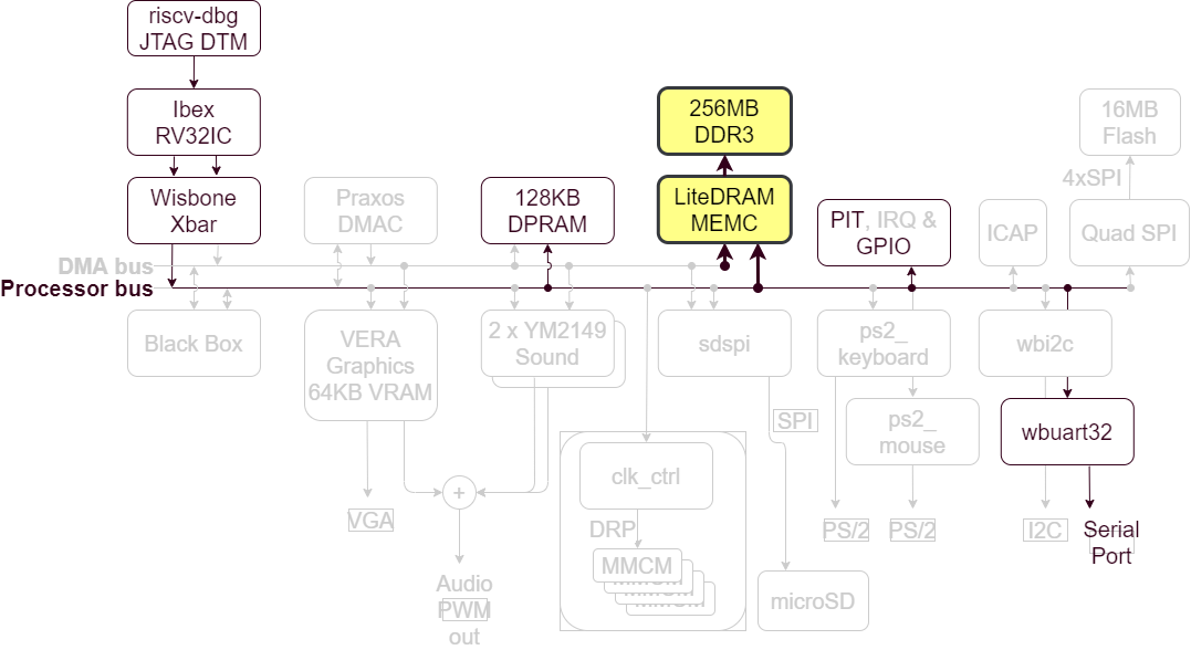
LiteDRAM in the BoxLambda Architecture.
Initially, the plan was to use Xilinx’s MIG (Memory Interface Generator) to generate a DDR Memory Controller for Boxlambda. At the time, that was (and maybe still is) the consensus online when I was looking for memory controller options for the Arty A7. Meanwhile, Reddit user yanangao suggested I take a look at project LiteX for a memory controller. I took the advice and started playing around a bit with Litex. One thing led to another and, long story short, BoxLambda now has a DDR memory controller based on LiteDRAM, a core of the LiteX project. If you’re interested in the longer story, read on.
Recap
This is a summary of the current state of BoxLambda. We have:
- An Ibex RISCV core, a Wishbone shared bus, a Debug Core, internal memory, a timer, two GPIO ports, and a UART core.
- A Picolibc-based standard C environment for software running on the Ibex RISCV core.
- Test builds running on Arty-A7-35T and Verilator.
- Automated testing on Verilator.
- OpenOCD-based Debug Access, both on FPGA and on Verilator.
- A Linux Makefile and Bender-based RTL build system.
LiteX and LiteDRAM
LiteX is an Open Source SoC Builder framework for FPGAs. You specify which CPU, memory, interconnect, and peripherals you want. The framework then generates the SoC and the software to go along with it. Here’s an example (with semi-randomly picked settings):
python3 digilent_arty.py --bus-standard wishbone --bus-data-width 32 --bus-interconnect crossbar --cpu-type rocket --integrated-sram-size 32768 --with-ethernet --with-sdcard --sys-clk-freq 50000000 --build --load

INFO:S7PLL:Creating S7PLL, speedgrade -1.
INFO:S7PLL:Registering Single Ended ClkIn of 100.00MHz.
INFO:S7PLL:Creating ClkOut0 sys of 50.00MHz (+-10000.00ppm).
INFO:S7PLL:Creating ClkOut1 eth of 25.00MHz (+-10000.00ppm).
INFO:S7PLL:Creating ClkOut2 sys4x of 200.00MHz (+-10000.00ppm).
INFO:S7PLL:Creating ClkOut3 sys4x_dqs of 200.00MHz (+-10000.00ppm).
INFO:S7PLL:Creating ClkOut4 idelay of 200.00MHz (+-10000.00ppm).
INFO:SoC:        __   _ __      _  __
INFO:SoC:       / /  (_) /____ | |/_/
INFO:SoC:      / /__/ / __/ -_)>  <
INFO:SoC:     /____/_/\__/\__/_/|_|
INFO:SoC:  Build your hardware, easily!
INFO:SoC:--------------------------------------------------------------------------------
INFO:SoC:Creating SoC... (2022-12-19 16:28:38)
INFO:SoC:--------------------------------------------------------------------------------
...
… and off it goes. That single command generates, synthesizes and loads the SoC onto your Arty A7.
LiteX is written in Migen, a Python-based tool that automates further the VLSI design process, to quote the website. At the heart of Migen sits FHDL, the Fragmented Hardware Description Language. FHDL is essentially a Python-based data structure consisting of basic constructs to describe signals, registers, FSMs, combinatorial logic, sequential logic etc. Here’s an example:
        aborted = Signal()        offset  = base_address >> log2_int(port.data_width//8)
        self.submodules.fsm = fsm = FSM(reset_state="CMD")        self.comb += [            port.cmd.addr.eq(wishbone.adr - offset),            port.cmd.we.eq(wishbone.we),            port.cmd.last.eq(~wishbone.we), # Always wait for reads.            port.flush.eq(~wishbone.cyc)    # Flush writes when transaction ends.        ]        fsm.act("CMD",            port.cmd.valid.eq(wishbone.cyc & wishbone.stb),            If(port.cmd.valid & port.cmd.ready &  wishbone.we, NextState("WRITE")),            If(port.cmd.valid & port.cmd.ready & ~wishbone.we, NextState("READ")),            NextValue(aborted, 0),        )        self.comb += [            port.wdata.valid.eq(wishbone.stb & wishbone.we),            If(ratio <= 1, If(~fsm.ongoing("WRITE"), port.wdata.valid.eq(0))),            port.wdata.data.eq(wishbone.dat_w),            port.wdata.we.eq(wishbone.sel),        ]
You can more or less see the Verilog equivalent. However, the fact that this is a Python data structure means that you have Python at your disposal as a meta-language to combine and organize these bits of HDL. This is a huge increase in abstraction and expressiveness, and it explains how LiteX can do what it does. The flexibility that LiteX provides in mixing and matching cores, core features, and interconnects, just can’t be achieved with vanilla SystemVerilog.
LiteX is not an all-or-nothing proposition. LiteX cores, such as the LiteDRAM memory controller, can be integrated into traditional design flows. That’s what I’ll be doing.
Why choose LiteDRAM over Xilinx MIG?
- LiteDRAM is open-source, scoring good karma points. All the benefits of open-source apply: Full access to all code, access to the maintainers, many eyeballs, the option to make changes as you please, submit bug fixes, etc.
- The LiteDRAM simulation model, the entire DDR test SoC, runs nicely in Verilator. That’s a must-have for me.
- The LiteDRAM core, configured for BoxLambda, is 50% smaller than the equivalent MIG core: 3016 LUTs and 2530 registers vs. 5673 LUTs and 5060 registers.
Generating a LiteDRAM core
LiteDRAM is a highly configurable core (because of Migen). For an overview of the core’s features, take a look at the LiteDRAM repository’s README file:
https://github.com/enjoy-digital/litedram/blob/master/README.md
You specify the configuration details in a .yml file. A Python script parses that .yml file and generates the core’s Verilog as well as a CSR register access layer for software.
Details are a bit sparse, but luckily example configurations are provided:
https://github.com/enjoy-digital/litedram/tree/master/examples
Starting from the arty.yml example, I created the following LiteDRAM configuration file for BoxLambda:
#This is a LiteDRAM configuration file for the Arty A7.
{    # General ------------------------------------------------------------------    "speedgrade": -1,          # FPGA speedgrade    "cpu":        "None",      # CPU type (ex vexriscv, serv, None) - We only want to generate the LiteDRAM memory controller, no CPU.    "memtype":    "DDR3",      # DRAM type    "uart":       "rs232",     # Type of UART interface (rs232, fifo) - not relevant in this configuration.
    # PHY ----------------------------------------------------------------------    "cmd_latency":     0,             # Command additional latency    "sdram_module":    "MT41K128M16", # SDRAM modules of the board or SO-DIMM    "sdram_module_nb": 2,             # Number of byte groups    "sdram_rank_nb":   1,             # Number of ranks    "sdram_phy":       "A7DDRPHY",    # Type of FPGA PHY
    # Electrical ---------------------------------------------------------------    "rtt_nom": "60ohm",  # Nominal termination    "rtt_wr":  "60ohm",  # Write termination    "ron":     "34ohm",  # Output driver impedance
    # Frequency ----------------------------------------------------------------    # The generated LiteDRAM module contains clock generation primitives, for its own purposes, but also for the rest    # of the system. The system clock is output by the LiteDRAM module and is supposed to be used as the main input clock    # for the rest of the system. I set the system clock to 50MHz because I couldn't get timing closure at 100MHz.    "input_clk_freq":   100e6, # Input clock frequency    "sys_clk_freq":     50e6, # System clock frequency (DDR_clk = 4 x sys_clk)    "iodelay_clk_freq": 200e6, # IODELAYs reference clock frequency
    # Core ---------------------------------------------------------------------    "cmd_buffer_depth": 16,    # Depth of the command buffer
    # User Ports ---------------------------------------------------------------    # We generate two wishbone ports, because BoxLambda has two system buses.    # Note that these are _classic_ wishbone ports, while BoxLamdba uses a _pipelined_ wisbone bus.    # A pipelined-to-classic wishbone adapter is needed to interface correctly to the bus.    # At some point it would be nice to have an actual pipelined wishbone frontend, with actual pipelining capability.    "user_ports": {        "wishbone_0" : {            "type":  "wishbone",            "data_width": 32, #Set data width to 32. If not specificied it defaults to 128 bits.            "block_until_ready": True,        },        "wishbone_1" : {            "type":  "wishbone",            "data_width": 32, #Set data width to 32. If not specificied it defaults to 128 bits.            "block_until_ready": True,        },    },
}
Some points about the above:
- The PHY layer, Electrical and Core sections I left exactly as-is in the given Arty example.
- In the General section, I set cpu to None. BoxLambda already has a CPU. We don’t need LiteX to generate one.
- In the Frequency section, I set sys_clk_freq to 50MHz. 50MHz has been the system clock frequency in the previous BoxLambda test builds as well. Also, I haven’t been able to close timing at 100MHz.
- In the User Ports section, I specified two 32-bit Wishbone ports. In the BoxLambda Architecture Diagram, you’ll see that BoxLambda has two system buses. The memory controller is hooked up to both.
I generate two LiteDRAM core variants from this configuration:
- For simulation:
litedram_gen artya7dram.yml --sim --gateware-dir sim/rtl --software-dir sim/sw --name litedram - For FPGA:
litedram_gen artya7dram.yml --gateware-dir arty/rtl --software-dir arty/sw --name litedram
The generated core has the following interface:
module litedram (
`ifndef SYNTHESIS      input  wire sim_trace, /*Simulation only.*/
`endif
	input  wire clk,
`ifdef SYNTHESIS  	input  wire rst,       /*FPGA only...*/
	output wire pll_locked,
	output wire [13:0] ddram_a,
	output wire [2:0] ddram_ba,
	output wire ddram_ras_n,
	output wire ddram_cas_n,
	output wire ddram_we_n,
	output wire ddram_cs_n,
	output wire [1:0] ddram_dm,
	inout  wire [15:0] ddram_dq,
	inout  wire [1:0] ddram_dqs_p,
	inout  wire [1:0] ddram_dqs_n,
	output wire ddram_clk_p,
	output wire ddram_clk_n,
	output wire ddram_cke,
	output wire ddram_odt,
	output wire ddram_reset_n,
`endif  	output wire init_done,  /*FPGA/Simulation common ports...*/
	output wire init_error,
	input  wire [29:0] wb_ctrl_adr,
	input  wire [31:0] wb_ctrl_dat_w,
	output wire [31:0] wb_ctrl_dat_r,
	input  wire [3:0] wb_ctrl_sel,
	input  wire wb_ctrl_cyc,
	input  wire wb_ctrl_stb,
	output wire wb_ctrl_ack,
	input  wire wb_ctrl_we,
	input  wire [2:0] wb_ctrl_cti,
	input  wire [1:0] wb_ctrl_bte,
	output wire wb_ctrl_err,
	output wire user_clk,
	output wire user_rst,
	input  wire [25:0] user_port_wishbone_0_adr,
	input  wire [31:0] user_port_wishbone_0_dat_w,
	output wire [31:0] user_port_wishbone_0_dat_r,
	input  wire [3:0] user_port_wishbone_0_sel,
	input  wire user_port_wishbone_0_cyc,
	input  wire user_port_wishbone_0_stb,
	output wire user_port_wishbone_0_ack,
	input  wire user_port_wishbone_0_we,
	output wire user_port_wishbone_0_err,
	input  wire [25:0] user_port_wishbone_1_adr,
	input  wire [31:0] user_port_wishbone_1_dat_w,
	output wire [31:0] user_port_wishbone_1_dat_r,
	input  wire [3:0] user_port_wishbone_1_sel,
	input  wire user_port_wishbone_1_cyc,
	input  wire user_port_wishbone_1_stb,
	output wire user_port_wishbone_1_ack,
	input  wire user_port_wishbone_1_we,
	output wire user_port_wishbone_1_err
);
Some points worth noting about this interface:
- A Wishbone control port is generated along with the two requested user ports. LiteDRAM CSR register access is done through this control port.
- All three Wishbone ports are classic Wishbone ports, not pipelined. There is no stall signal.
- The Wishbone port addresses are word addresses, not byte addresses.
- The LiteDRAM module takes an external input clock (clk) and generates a 50MHz system clock (user_clk). The module contains a clock generator.
- On FPGA, the LiteDRAM module takes an asynchronous reset (rst) and provides a synchronized reset (user_rst). The module contains a reset synchronizer.
Integrating the LiteDRAM core
Litedram_wrapper
I created a litedram_wrapper module around litedram.v:
This wrapper contains:
- byte-to-word address adaptation on all three Wishbone ports.
- Pipelined-to-Classic Wishbone adaptation. The adapter logic comes straight out of the Wishbone B4 spec section 5.2, Pipelined master connected to standard slave. The stall signal is used to avoid pipelining:
/*Straight out of the Wishbone B4 spec. This is how you interface a classic slave to a pipelined master. *The stall signal ensures that the STB signal remains asserted until an ACK is received from the slave.*/ assign user_port_wishbone_p_0_stall = !user_port_wishbone_p_0_cyc ? 1'b0 : !user_port_wishbone_c_0_ack;
How long to STB?
One Rookie mistake I made early on was to just set the Wishbone stall signal to 0. I figured that, as long as I didn’t generate multiple outstanding transactions, that should work just fine. That’s not the case, however. Wishbone transactions to the LiteDRAM core would just block. The reason is that in classic Wishbone, STB has to remain asserted until an ACK or ERR is signaled by the slave. Pipelined Wishbone doesn’t work that way. In pipelined Wishbone, as long as the slave is not stalling, a single access STB only remains asserted for one clock cycle.
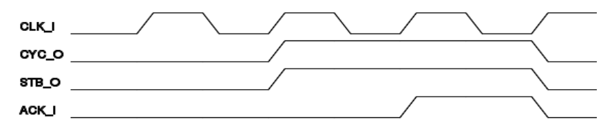
Classic Wishbone transaction (Illustration taken from Wishbone B4 spec).
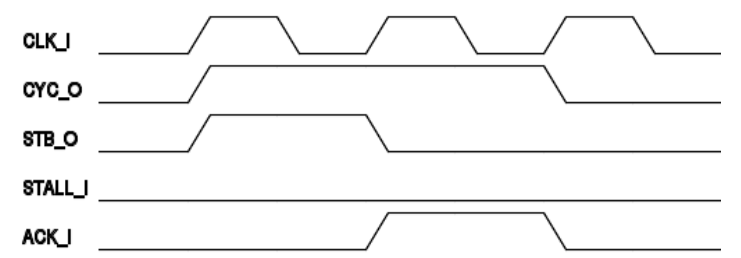
Pipelined Wishbone transaction - single access (Illustration taken from Wishbone B4 spec).
Hence the pipelined-to-classic Wishbone adapter in litedram_wrapper.
More Wishbone Issues: Core2WB and WB_Interconnect_SharedBus
With the litedram_wrapper in place, Wishbone transactions still weren’t working properly. Waveform analysis shows that, from the point of view of litedram_wrapper, the Wishbone Bus Master wasn’t well-behaved. That problem could either come from the Ibex memory-interface-to-wishbone adapter, core2wb.sv, or the Wishbone shared bus implementation used by the test build, wb_interconnect_shared_bus.sv, or both.
This is the Ibex Memory Interface specification:
https://ibex-core.readthedocs.io/en/latest/03_reference/load_store_unit.html#load-store-unit
There are two such interfaces. One for data, one for instructions.
The job of core2wb is to adapt that interface to a pipelined Wishbone bus master interface. That Wishbone bus master in turn requests access to the shared bus. It’s up to wb_interconnect_shared_bus to grant the bus to one of the requesting bus masters and direct the transaction to the selected slave. If either one of those modules has a bug, that will result in an incorrectly behaving bus master, from the point of view of the bus slave.
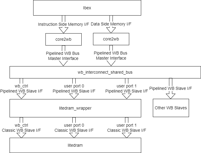
From Ibex to LiteDRAM.
core2wb.sv and wb_interconnect_shared_bus.sv are part of the ibex_wb repository. The ibex_wb repository no longer appears to be actively maintained. I looked long and hard at the implementation of the two modules and ultimately decided that I couldn’t figure out the author’s reasoning. I decided to re-implement both modules:
- Core2wb has two states: Idle and Transaction Ongoing. In the Idle state, when Ibex signals a transaction request (core.req), the Ibex memory interface signals get registered, a single access pipelined Wishbone transaction is generated and core2wb goes to Transaction Ongoing state. When a WB ACK or ERR response is received, core2wb goes back to idle. While Transaction Ongoing state, the memory interface grant (gnt) signal is held low, so further transaction requests are stalled until core2wb is idle again Multiple outstanding transactions are currently not supported. I hope to add that capability someday.
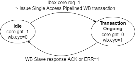
Core2WB State Diagram.
- WB_interconnect_shared_bus also has two states: In the Idle state, a priority arbiter monitors the CYC signal of participating Bus Masters. When one or more Bus Masters assert CYC, the arbiter grants access to the lowest order Bus Master and goes to Transaction Ongoing state. When that Bus Master de-asserts CYC again, we go back to Idle state. Slave selection and forwarding of WB signals is done with combinatorial logic.
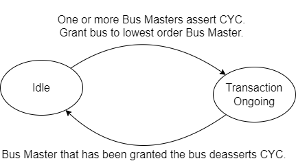
WB_Interconnect_Shared_Bus State Diagram.
With those changes in place, Ibex instruction and data transactions to LiteDRAM are working fine.
ddr_test_soc
/projects/ddr_test/rtl/ddr_test_soc.sv has the test build’s top-level. It’s based on the previous test build’s top-level, extended with the LiteDRAM wrapper instance.
  litedram_wrapper litedram_wrapper_inst (
	.clk(ext_clk100), /*100MHz External clock is input for LiteDRAM module.*/    .rst(~ext_rst_n), /*External reset goes into a reset synchronizer inside the litedram module. The output of that synchronizer is sys_rst.*/    .sys_clk(sys_clk), /*LiteDRAM outputs 50MHz system clock...*/
	.sys_rst(sys_rst), /*...and system reset.*/
	.pll_locked(pll_locked),
`ifdef SYNTHESIS
	.ddram_a(ddram_a),
	.ddram_ba(ddram_ba),
	.ddram_ras_n(ddram_ras_n),
	.ddram_cas_n(ddram_cas_n),
	.ddram_we_n(ddram_we_n),
	.ddram_cs_n(ddram_cs_n),
	.ddram_dm(ddram_dm),
	.ddram_dq(ddram_dq),
	.ddram_dqs_p(ddram_dqs_p),
	.ddram_dqs_n(ddram_dqs_n),
	.ddram_clk_p(ddram_clk_p),
	.ddram_clk_n(ddram_clk_n),
	.ddram_cke(ddram_cke),
	.ddram_odt(ddram_odt),
	.ddram_reset_n(ddram_reset_n),
`endif
	.init_done(init_done_led),
	.init_error(init_err_led),
	.wb_ctrl_adr(wbs[DDR_CTRL_S].adr),
	.wb_ctrl_dat_w(wbs[DDR_CTRL_S].dat_m),
	.wb_ctrl_dat_r(wbs[DDR_CTRL_S].dat_s),
	.wb_ctrl_sel(wbs[DDR_CTRL_S].sel),    .wb_ctrl_stall(wbs[DDR_CTRL_S].stall),
	.wb_ctrl_cyc(wbs[DDR_CTRL_S].cyc),
	.wb_ctrl_stb(wbs[DDR_CTRL_S].stb),
	.wb_ctrl_ack(wbs[DDR_CTRL_S].ack),
	.wb_ctrl_we(wbs[DDR_CTRL_S].we),
	.wb_ctrl_err(wbs[DDR_CTRL_S].err),
  /*Eventually we're going to have two system buses, but for the time being, to allow testing,   *we hook up both user ports to our one shared bus.   *Both ports address the same 256MB of DDR memory, one at base address 'h40000000, the other at 'h50000000.*/
	.user_port_wishbone_p_0_adr(wbs[DDR_USR0_S].adr),
	.user_port_wishbone_p_0_dat_w(wbs[DDR_USR0_S].dat_m),
	.user_port_wishbone_p_0_dat_r(wbs[DDR_USR0_S].dat_s),
	.user_port_wishbone_p_0_sel(wbs[DDR_USR0_S].sel),
	.user_port_wishbone_p_0_stall(wbs[DDR_USR0_S].stall),
	.user_port_wishbone_p_0_cyc(wbs[DDR_USR0_S].cyc),
	.user_port_wishbone_p_0_stb(wbs[DDR_USR0_S].stb),
	.user_port_wishbone_p_0_ack(wbs[DDR_USR0_S].ack),
	.user_port_wishbone_p_0_we(wbs[DDR_USR0_S].we),
	.user_port_wishbone_p_0_err(wbs[DDR_USR0_S].err),

	.user_port_wishbone_p_1_adr(wbs[DDR_USR1_S].adr),
	.user_port_wishbone_p_1_dat_w(wbs[DDR_USR1_S].dat_m),
	.user_port_wishbone_p_1_dat_r(wbs[DDR_USR1_S].dat_s),
	.user_port_wishbone_p_1_sel(wbs[DDR_USR1_S].sel),
	.user_port_wishbone_p_1_stall(wbs[DDR_USR1_S].stall),
	.user_port_wishbone_p_1_cyc(wbs[DDR_USR1_S].cyc),
	.user_port_wishbone_p_1_stb(wbs[DDR_USR1_S].stb),
	.user_port_wishbone_p_1_ack(wbs[DDR_USR1_S].ack),
	.user_port_wishbone_p_1_we(wbs[DDR_USR1_S].we),
	.user_port_wishbone_p_1_err(wbs[DDR_USR1_S].err)  );
Clock and Reset generation is now done by LiteDRAM. LiteDRAM accepts the external clock and reset signal and provides the system clock and synchronized system reset. Previous BoxLambda test builds had a separate Clock-and-Reset-Generator instance for that.
In this test build, both user ports are hooked up to the same shared bus. That doesn’t make a lot of sense of course. I’m just doing this to verify connectivity over both buses. Eventually, BoxLambda is going to have two buses and LiteDRAM will be hooked up to both.
LiteDRAM Initialization
When the litedram_gen.py script generates the LiteDRAM Verilog core (based on the given .yml configuration file), it also generates the core’s CSR register accessors for software:
- For FPGA: https://github.com/epsilon537/boxlambda/tree/develop/components/litedram/arty/sw/include/generated
- For simulation: https://github.com/epsilon537/boxlambda/tree/develop/components/litedram/sim/sw/include/generated
The most relevant files are csr.h and sdram_phy.h. They contain the register definitions and constants used by the memory initialization code. Unfortunately, these accessors are not the same for the FPGA and the simulated LiteDRAM cores. We’re going to have to use separate software builds for FPGA and simulation.
Sdram_init()
Sdram_phy.h also contains a function called init_sequence(). This function gets invoked as part of a more elaborate initialization function called sdram_init(). Sdram_init() is not part of the generated code, however. It’s part of sdram.c, which is part of liblitedram, which is part of the base Litex repository, not the LiteDRAM repository:
https://github.com/epsilon537/litex/tree/master/litex/soc/software/liblitedram
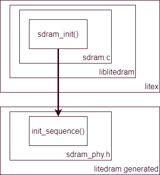
sdram_init() vs. init_sequence().
It’s not clear to me why the liblitedram is not part of the LiteDRAM repository, but’s not a big deal. I integrated the sdram_init() function from liblitedram in the BoxLambda code base and it’s working fine.
To get things to build, I added Litex as a git submodule, to get access to liblitedram. I also tweaked some CPPFLAGS and include paths. The resulting Makefiles are checked-in here:
- FPGA: https://github.com/epsilon537/boxlambda/blob/master/sw/projects/ddr_test/fpga/Makefile
- Sim: https://github.com/epsilon537/boxlambda/blob/master/sw/projects/ddr_test/sim/Makefile
It’s worth noting that liblitedram expects a standard C environment, which I added in the previous BoxLambda update.
DDR Test
The DDR test program is located here:
https://github.com/epsilon537/boxlambda/blob/master/sw/projects/ddr_test/ddr_test.c
The program boots from internal memory. It invokes sdram_init(), then performs a memory test over user port 0, followed by user port 1. Finally, the program verifies CPU instruction execution from DDR by relocating a test function from internal memory to DDR and branching to it.
The memory test function used is a slightly modified version of the memtest() function provided by Litex in liblitedram.
Relevant Files
- https://github.com/enjoy-digital/litex/blob/master/litex/soc/software/liblitedram/sdram.c
- https://github.com/epsilon537/boxlambda/blob/master/components/litedram/common/rtl/litedram_wrapper.sv
- https://github.com/epsilon537/boxlambda/blob/master/components/litedram/arty/rtl/litedram.v
- https://github.com/epsilon537/boxlambda/blob/master/components/litedram/sim/rtl/litedram.v
- https://github.com/epsilon537/boxlambda/blob/master/components/litedram/artya7dram.yml
- https://github.com/epsilon537/boxlambda/blob/master/projects/ddr_test/rtl/ddr_test_soc.sv
- https://github.com/epsilon537/boxlambda/blob/master/sw/projects/ddr_test/ddr_test.c
- https://github.com/epsilon537/boxlambda/blob/master/sw/projects/ddr_test/fpga/Makefile
- https://github.com/epsilon537/boxlambda/blob/master/sw/projects/ddr_test/sim/Makefile
- https://github.com/epsilon537/boxlambda/blob/master/components/litedram/arty/sw/include/generated/csr.h
- https://github.com/epsilon537/boxlambda/blob/master/components/litedram/arty/sw/include/generated/sdram_phy.h
- https://github.com/epsilon537/boxlambda/blob/master/components/litedram/sim/sw/include/generated/csr.h
- https://github.com/epsilon537/boxlambda/blob/master/components/litedram/sim/sw/include/generated/sdram_phy.h
Try It Out
Repository setup
- Install the Prerequisites.
- Get the BoxLambda repository:
git clone https://github.com/epsilon537/boxlambda/
cd boxlambda
- Switch to the enter_litedram tag:
git checkout enter_litedram
- Set up the repository. This initializes the git submodules used and builds picolibc for BoxLambda:
make setup
Build and Run the DDR Test Image on Verilator
- Build the test project:
cd projects/ddr_test
make sim
- Execute the generated verilator model in interactive mode:
cd generated
./Vmodel -i
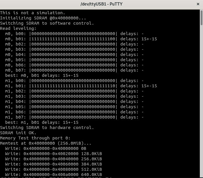
- You should see something like this:
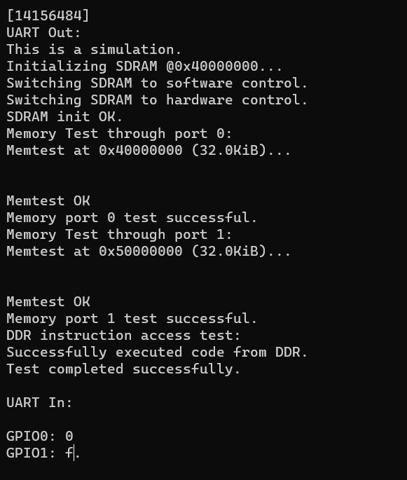
DDR Test on Verilator.
Build and Run the DDR Test Image on Arty A7
- If you’re running on WSL, check BoxLambda’s documentation On WSL section.
- Build the test project:
cd projects/ddr_test
make impl
- Connect a terminal program such as Putty or Teraterm to Arty’s USB serial port. Settings: 115200 8N1.
- Run the project:
make run
- Verify the test program’s output in the terminal. You should see something like this:
DDR Test on Arty A7-35T.
Other Changes
-
To minimize the differences with the Arty A7-35T (Little BoxLambda), I decided to use the Arty A7-100T rather than the Nexys A7 as the Big BoxLambda variant.
-
I noticed belatedly that I didn’t create a constraint for the tck JTAG clock, so no timing analysis could be done on the JTAG logic. I added the following to the .xdc constraints file. Vivado’s timing analysis is much happier now.
#This is the JTAG TCK clock generated by the BSCANE2 primitive.
#Note that the JTAG top-level ports (incl. TCK) are not used in a synthesized design. They are driven by BSCANE2 instead.
create_clock -period 1000.000 -name dmi_jtag_inst/i_dmi_jtag_tap/tck_o -waveform {0.000 500.000} [get_pins dmi_jtag_inst/i_dmi_jtag_tap/i_tap_dtmcs/TCK]
- I have merged the development branch to the master branch. Going forward, I intend to do that every time I put down a release label for a new Blog post.
Interesting Links
https://github.com/antonblanchard/microwatt: An Open-Source FPGA SoC by Anton Blanchard using LiteDRAM. I found it helpful to look at that code base to figure out how to integrate LiteDRAM into BoxLambda.
Discussions
Become a Hackaday.io Member
Create an account to leave a comment. Already have an account? Log In.