 kaimac
CPU
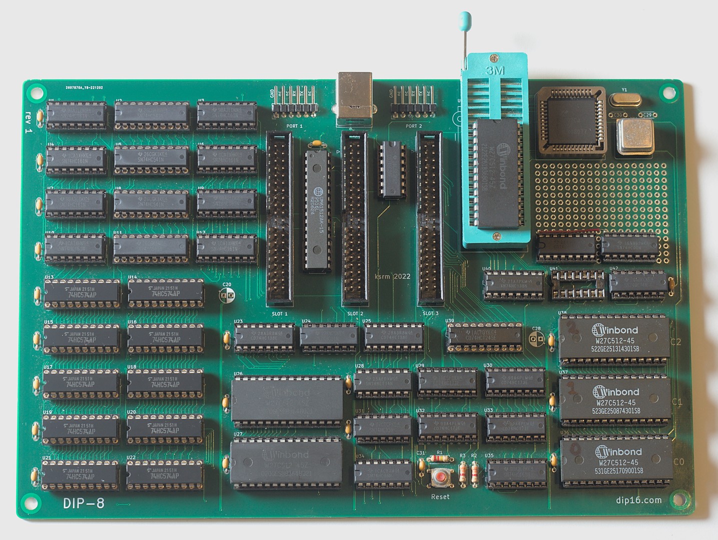
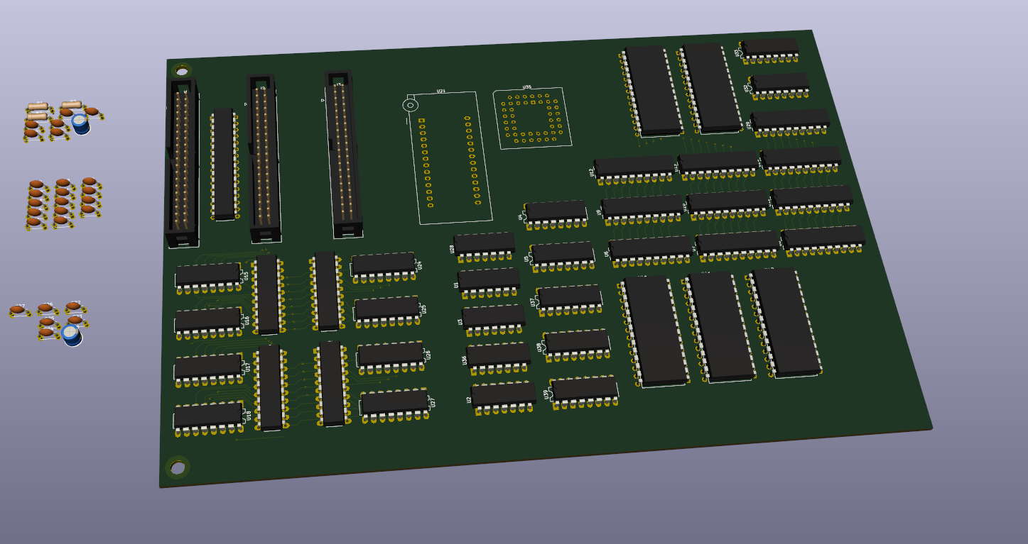
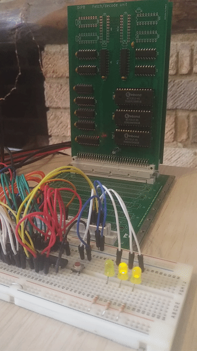
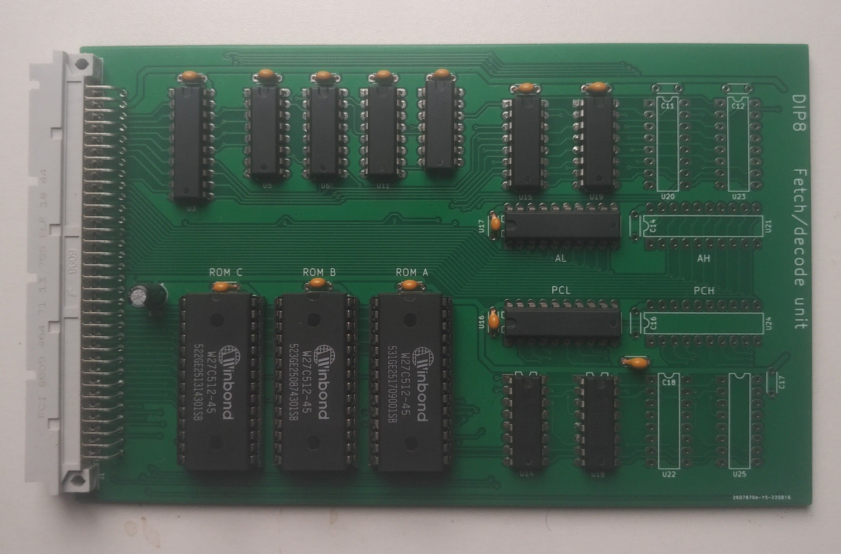
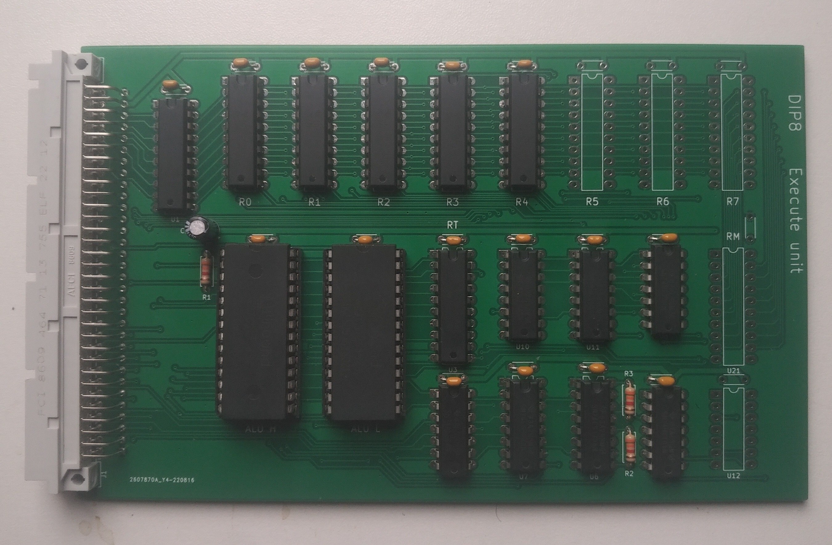
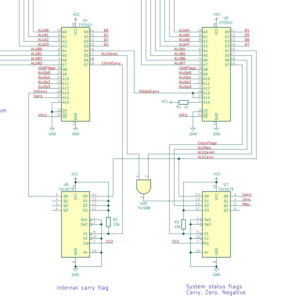
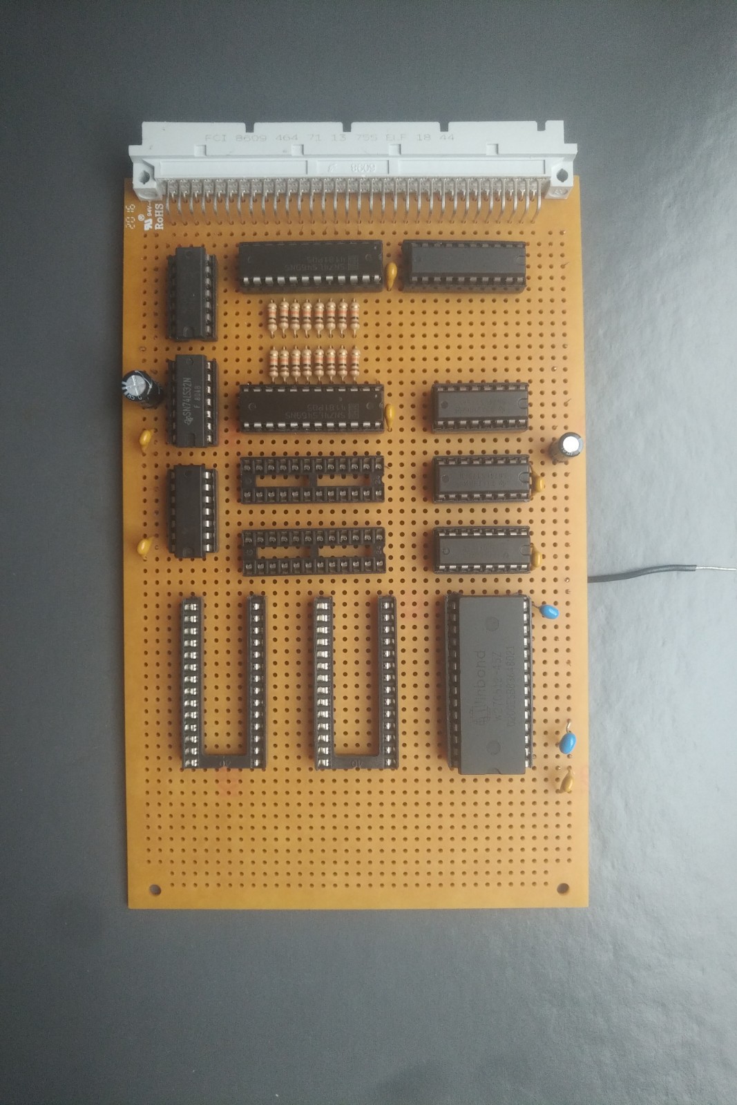
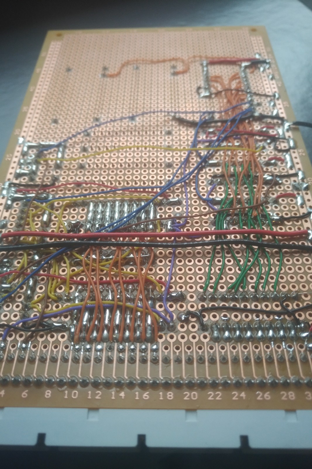
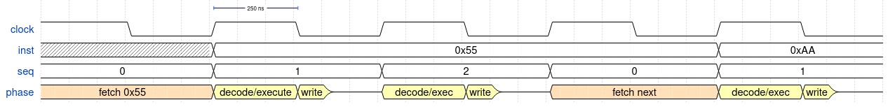
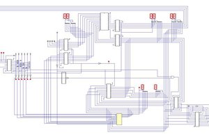
As my first CPU design to leave my notebook, I wanted to keep things simple, so I'm using EEPROMs as simple programmable logic devices. Two 64KB devices make up the ALU, and another three decode instructions into 23 control lines. The design is faster than it might sound, thanks to the existence of the Winbond W27C512-45, a 45 ns EEPROM which is readily available (on eBay!) and I think the fastest EEPROM of its size.
Using ROMs for instruction decoding allows for a featureful instruction set while the rest of the hardware is quite simple. There are some 16-bit operations, a load of different addressing modes (including stack-relative for higher-level languages), and the ALU operations can work on registers or values in memory.
- 6x general-purpose 8-bit registers: X, Y, BH, BL, CH, CL
- BH/BL/CH/CL form two 16-bit register pairs (B, C)
- 16-bit stack pointer and program counter
- ROM-based ALU can perform add, subtract, and, or, xor, rotate right, signed and unsigned comparisons
- Carry, zero and negative flags for conditional jumps
- No interrupts
System
- 8-bit data bus, 16-bit address bus
- 4 MHz clock
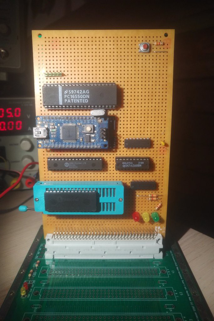
- Serial interface
Software
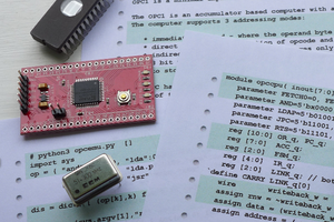
- Development tools (assembler, emulator) written in Python
- I have a plan for a cooperatively-multitasked operating system
- Ultimate plan is to design a high(ish) level language and write a compiler
 Ed S
Ed S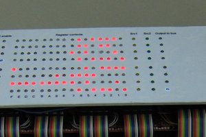
 Pavel
Pavel
Nice project!