Eric Ljungquist
The finished project demo video:
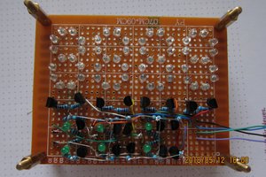
The above demo shows the decoder hooked up to a counter circuit on the left breadboard that generates a up counting 4-bit binary signal. The output of the decoder is feed to a homemade seven segment display on the perfboard on the right. The transistors on the display board are just drivers for the LEDs
At the start of this project I decided I wanted to decode full 4-bit binary 0 to 15 into hexadecimal 0 to F. There are a few designs out there such as the 74LS47 to convert binary BCD to decimal 0-9 but I personally wanted the full range of 0 to 15 to display. With what I wanted the output to be in mind, I mapped the corresponding input and output values on paper. Karnaugh maps were then used to simplify output logic. I unfortunately can't find the papers where I did this simplification on so I can't include an image of the work. If I get some time I will try to come back to this and redo the work for a series of images.
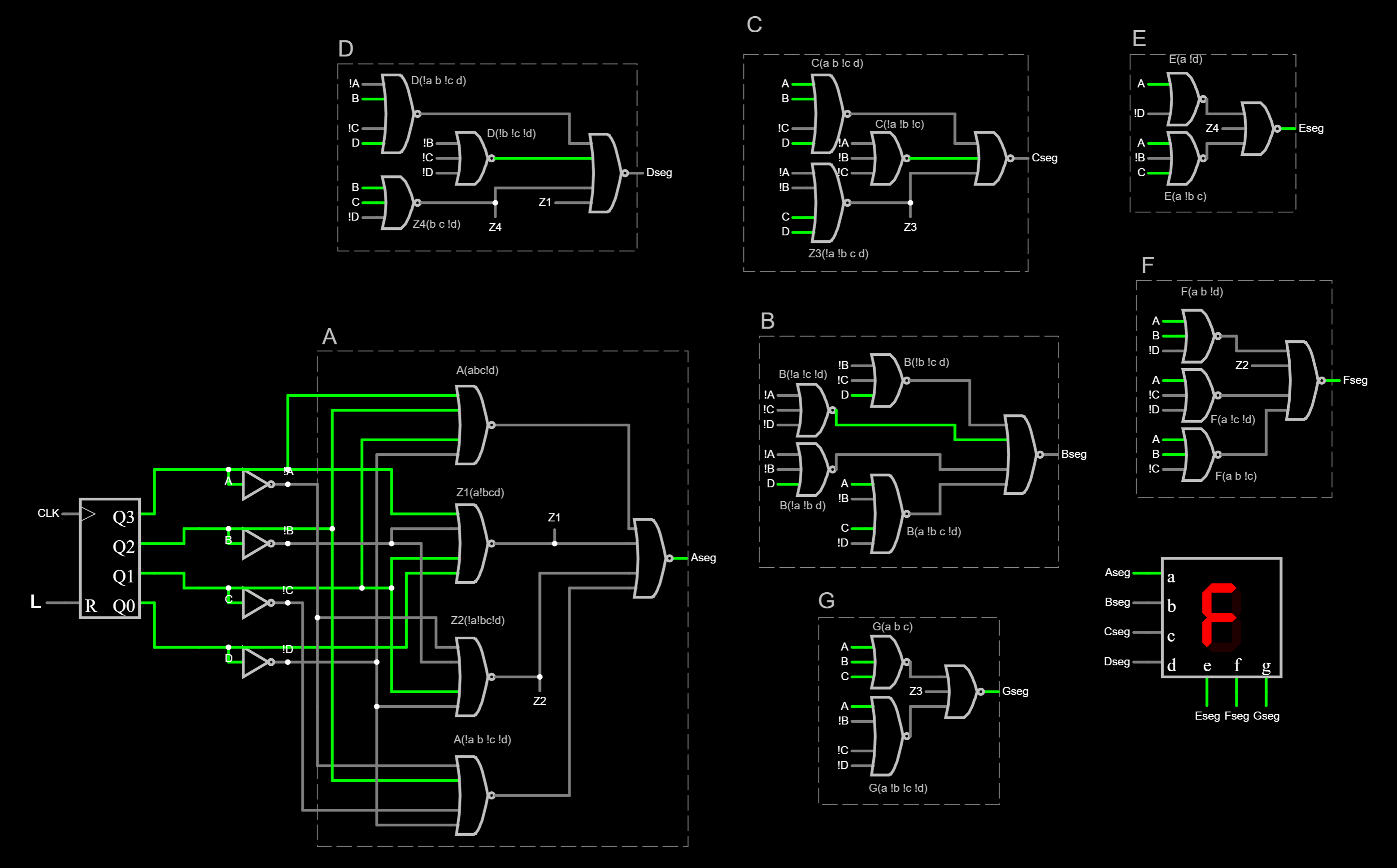
After simplifying the logic, the circuit was prototyped in Falstad's CircuitJS. You can click the link below to load the live demo of the above image.
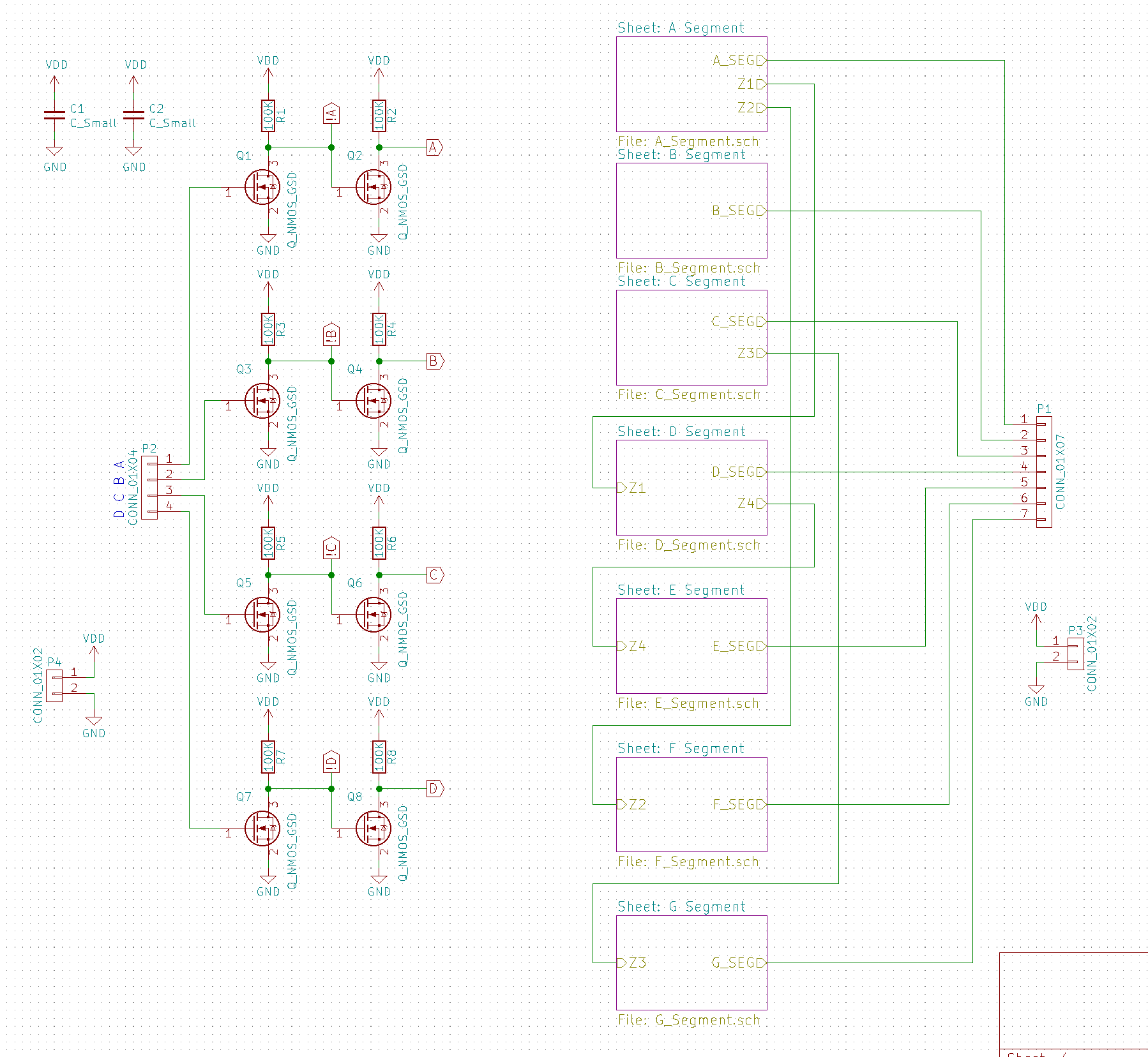
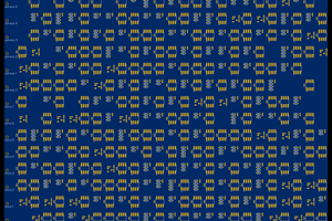
The same logic view was then recreated in KiCad. Adding connectors and expanding logic gates into their corresponding NMOS logic circuits. To reduce clutter on the main sheet, each segments logic was given its own sheet.

Each segment sheet then just contains the wiring and NOR gates.

All the NOR gates are the same. The only difference between gates is the number of inputs.
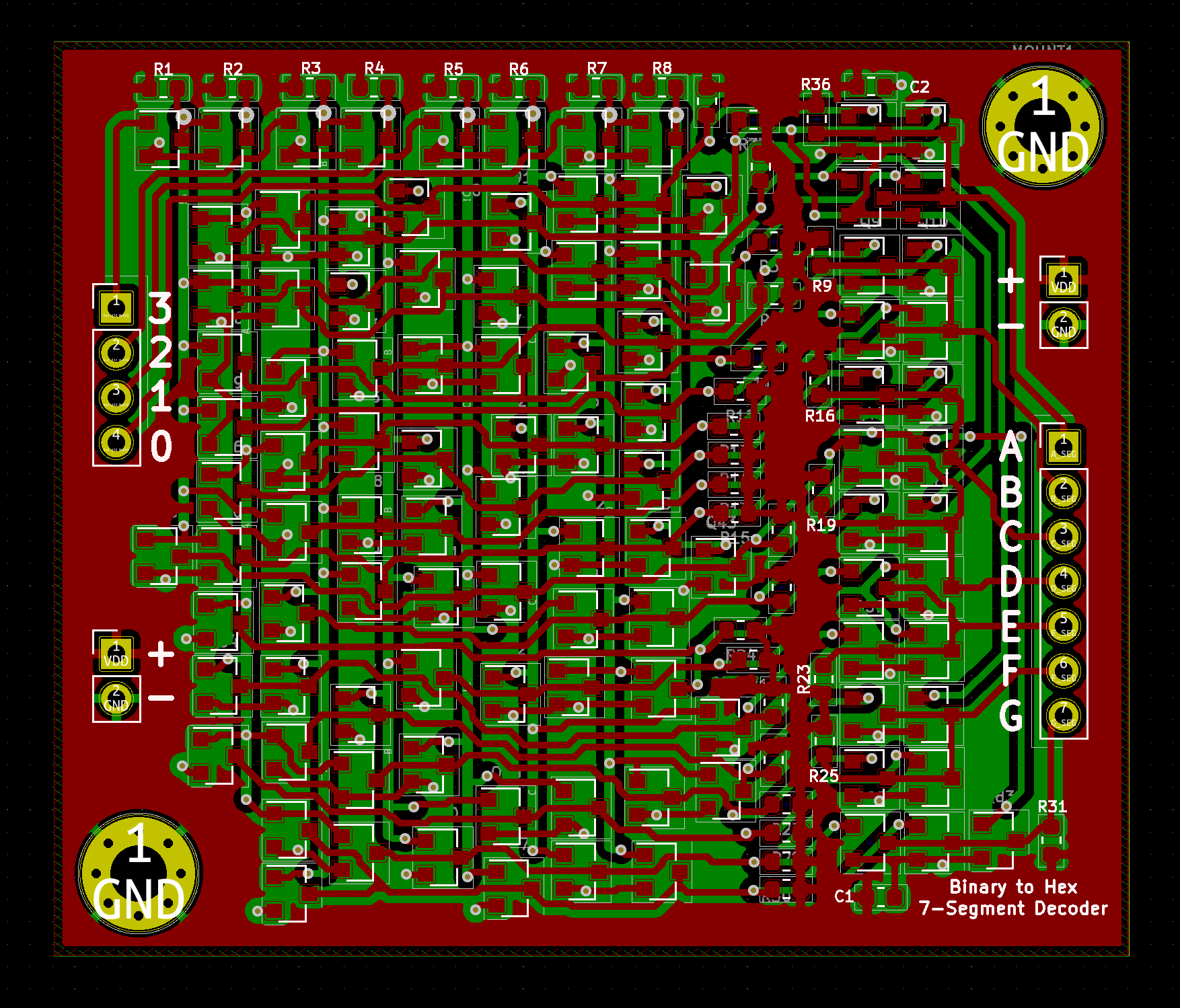

After the schematic was finished, the design was imported into KiCad's Pcbnew. From there is was just a grind to try to fit all the transistors in as little space as possible. I decided to put the input buffers along the top edge of the board with the output signals running vertically along the back copper layer. The first layer of NOR gates are right below the input buffers and run horizontally along the top copper layer. The inputs of the NOR gates tap into the required inputs through vias to the back side. Since routing the second layer of NOR gates wasn't much of a layout issue, they were just placed in a column in the remaining space to the right.
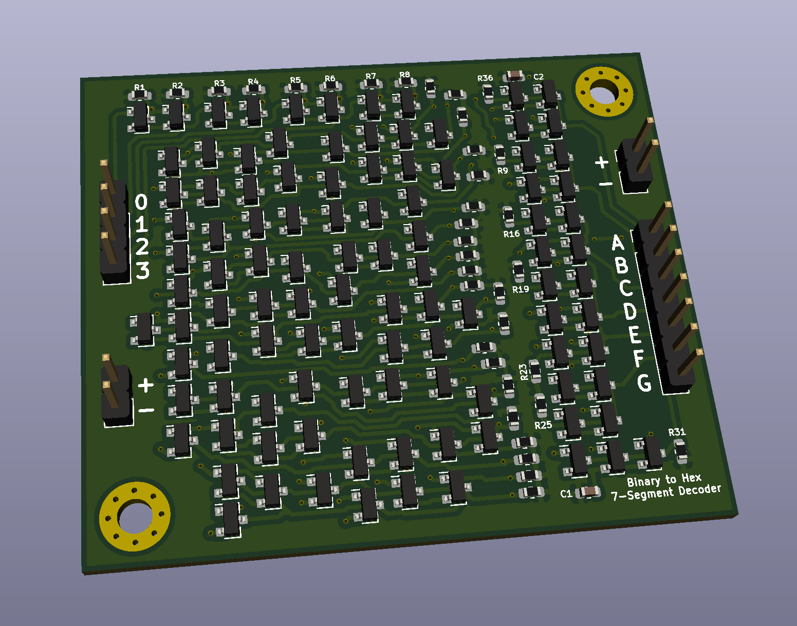


I then had the boards created at OSHPark and then soldered all components to the board. I did have one bum transistor but after solving that, luckily the board worked without needing adjustments. The only issue left over with the layout is that I numbered the input pins wrong. Input pin 0 should be the bottom pin and it should count up from there.
 Tim
Tim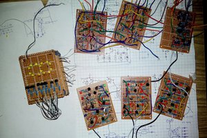
 Pavel
Pavel
 Dr. Cockroach