 Dave Collins
IT WORKS!!
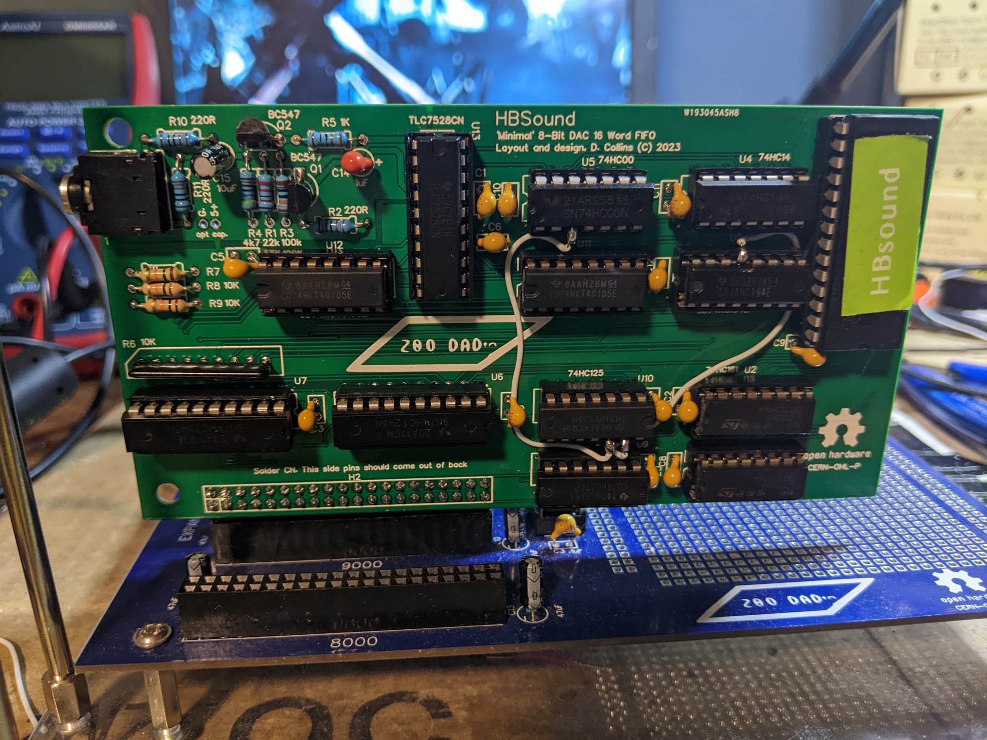
Board review
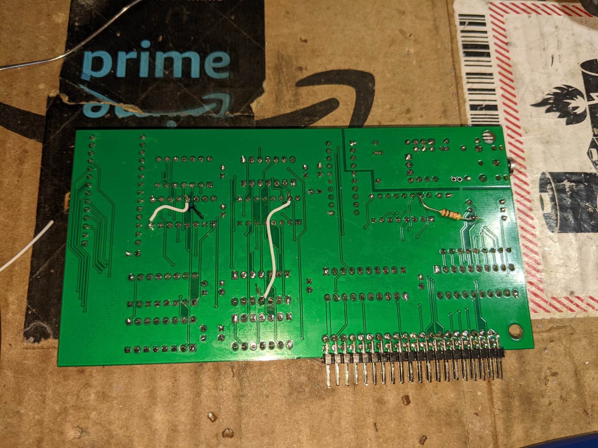
So after receiving the boards back from the sponsor PCBWay, which took about a week. I was very pleased with the build quality, which continues to exceed my standards for what a prototype board should look like. I have no doubt in saying, that these boards hold up even with the lowest cost build options. In fact when mounting the edge connector on the board I made a mistake and had to manually remove the connector to solder a new one, and was concerned because usually there is some damage to the solder masking around the rework area on prototypes with manual de-soldering. But to my surprise, there was only mild wear on the masking which needed to be cleaned up by applying some nail varnish (but not much) before re-populating the connector in the board. This is a huge plus if you are working on a prototype and find the need to de-solder a large part but do not have a fancy de-soldering pump. Other services use much less consistency in the amount and quality of mask that is applied. This time I did the bog standard green which is what comes with the low cost option on many other services and I am pleased to say even on economy masking, the level of quality is really there, this may be due to multiple coats or just a slower application; whatever the case I was very happy with the results.
Full disclosure disclaimer: PCBWay is sponsoring the prototyping by providing them for free. I received no money to make these statements, and my observations are my own. Additionally PCBWay has not requested to review or change any of my statements prior to making them.
HB6809 In the news, the HBSound and more:
About a week ago I did a YouTube video reviewing the design of the control unit on my sound card, This was kind of a follow up to the last journal entry. I also did some block diagrams in my lab notebook. I also updated everything in the files section with the newest schematic, high resolution PCB rendering files as well as a excel spread sheet breaking out the math for the counts in the state machine .HEX (which is also included). I'd like to test the new gerbers out by having them made to make sure that they are working which may be a week or two out. I don't anticipate any of the issue with the design updates (however silly mistakes can happen).
Another thing of note: a small clone of the Jeff Tranter / Grant Searle (and i guess now me, Lol) 6809 design was made by hardware hacker antibyte! This thing is a tiny 6809 single board computer (with a very useful expansion port). The parts were sourced to be what is generally available from PCB assemblers IE, you should be able to just order one and have it assembled (with acceptation of the through hole parts that is!) The design uses one of the expansion spaces in my design to expand the rom space; I very much love this idea! I think I will build a RAM / ROM expansion for my computer based off of this. The clock circut and powering is different (he integrates a USB to serial chip, as well as other useful bits (a baud-rate generator). I also had planned to re-work the clock oscillator on the computer to make use of faster 63c09 chips -- this might require a redesign of the motherboard -- more on that later!
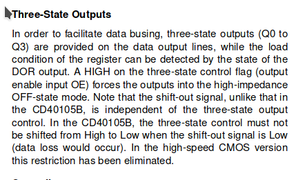
Issues with the CD 74HC40105 datasheet:
I had encountered issues with the modern 10405 FIFO equivalents from TI mainly with the /OE operation and specifically how it was documented in the datasheet.
In the CD74HC40105 datasheet the /OE pin is documented this way:
with the following block diagram:
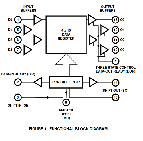
see what is missing here - no mention is made of the OE line at all. To add insult to injury, this is the logic diagram:
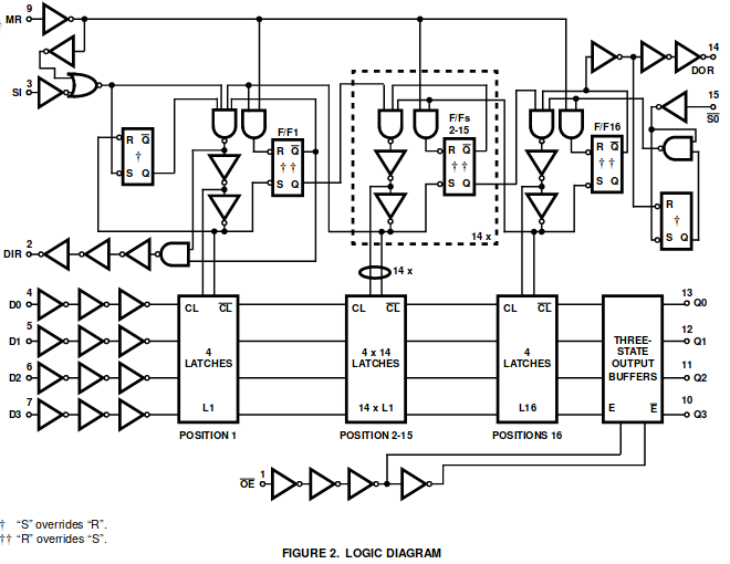
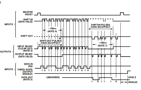
This seems to suggest the /OE line only affects the Q0 - Q3 outputs. Even the master timing diagram doesn't seem to show any thing different:
However upon building up the prototype, I discovered that the flags from the FIFO's were not updating while the /OE pin was set high. This is a issue i never tested for on the breadboard when I was working with the part during the design phase, as the datasheet seemed to indicate that those outputs would always be representative of the status of the register.
Imagine my surprise, when low and behold I was having issues with this specific thing. I suspect this has to do with the changes to prevent data corruption, but unless somebody de-caps a CD74HCT40105 and looks at the logic, we will have to wonder.
This causes a issue with my design:
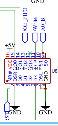
I run the /OE signal directly from the control register, so when the register is set to stop the outputs on the FIFO they lock in a state which makes them unusable for the current flags register on my sound card.
To resolve the issue I re-purposed a tri-state buffer from the design which was terminated to +5V:
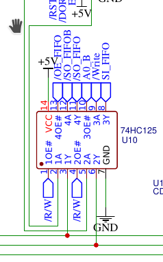
Now the signal from the shift out clock (which I re-named SO_FIFOB) is gated by the /OE_FIFO signal. I also tied the output of the buffer to +5v through a 10k resistor in order to prevent the clock state from floating when it is disabled. Additionally I tied the output enable line to ground on the FIFO's to lock the outputs to always on.
After making the changes, I tested with a few pokes in basic and everything is performing as planned.
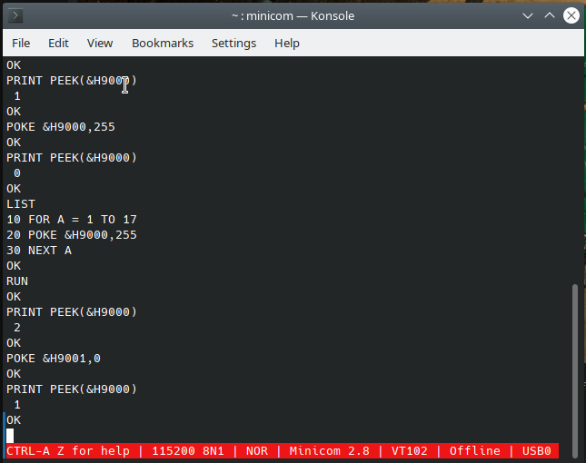
It doesn't look like a lot but this is actually a complete proof of function. Sending a poke to location 9001 (off screen) a value of 7, we send a 111 to the control register. This disables the DAC Clock and sets the clock to 7.2kHZ. Peeking at the address space of slot 9000 we see the register returns a 1, this means that the FIFO is showing that it is empty and has no more data to output. DOR is LOW, DIR is HIGH but they are inverted by the NAND gates so the returned value is 1. If we send 1 byte to the FIFO with another poke to 9000, and then peek at the address again we see a 0. This means the DIR / DOR are both HIGH, but are inverted and so the return value is 0. If we run the short program to send a bunch of bytes to the address we flood the FIFO and it overflows. Since it is full if we peek at the address we see that it is returning 2, this means that DOR is HIGH, and DIR is LOW as the signals are inverted by the NAND gate. If we again poke 9001 and set the control register to 0, this turns the DAC CLOCK back on and sets the CLOCK to its fastest speed of 32kHz. Peeking at the address again we can see the FIFO is emptied, and the flags are reading 1 again.
Scope analysis:
Taking a look at the NAND gate that is the output of the OR function:
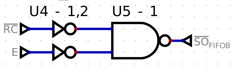
We can see this takes the output of the state machine and does a OR operation on it and the system clock 'E', so that when both signals go LOW the /SO_FIFOB signal is LOW. This is exactly what we want as this grantees the shift out happens only on the falling edge of the system clock (If you would like this is further explained in the last entry in this space).
If we probe this output with an oscilloscope, and run some basic pokes:
We can see that the scope shows the clock changing frequency:
 |  |  |
 |  |  |
I also did a test of the edges of the clock which show significant ringing, some of this is due to the poor ground point for the probe but also could be an impedance mismatch on the trace and bodge from the output of the gate. The ringing is not anything I think I need to be concerned about as the speed of the edges are slow enough this is likely not to matter, additionally the amplitude is not above (or below) the switching threshold of the input. If I have issues at speed I can simply install a termination resistor in line with the output (or input).
Whats next?
I need to work on a test program that loads data at speed, as Microsoft Enhanced Basic is not fast enough to update the FIFO to produce anything more than a small 200Hz square wave (which ill save your ears from). I will definitely do something in assembly to demonstrate the card by playing a digital sample. I want to as stated before order some replacement PCB's after knocking together a quick memory expansion (possibly in the prototype area). It is Ideal for this as it is going to be near all the signals I will need. I'll be switching to a larger, electrically erasable EEPROM and a larger RAM chip. Additionally I have a ZX81 I am restoring that takes up some of my time as well, you can follow along with the progress on my 'hack a day pages' blog here. I am also working on a new integrated terminal board in my notebook, which I'm not quite ready to share all of but suffice to say I am looking at a few modern QPLD socket-able serial chips from maximum integrated. Over the next week or so the focus will be on getting an assembly tool-chain set up and writing code for the sound card, so watch this space for updates. Thanks for taking the time to read about my little projects, and thanks again to PCB way without their support projects like this would take considerably longer. If you have any questions feel free to drop me a line I will try my best to answer.
Discussions
Become a Hackaday.io Member
Create an account to leave a comment. Already have an account? Log In.