The goal of this project is show the possibilities of the RP2040. It is a new microcontroller from Raspberry Pi based on an Arm Cortex M0+ with a dual-core processor and with a new programmable peripheral named PIO.
Diagram overview
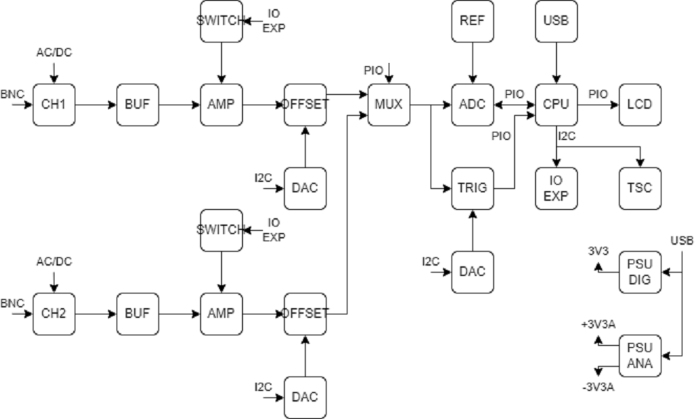
In this diagram we see all the elements of the oscilloscope.
- The power supply comes from the USB and is regulated independently for the analog and digital parts.
- Each analog stage is made up of 3 op amps, a gain selector and a DAC for the offset. The selection between AC/DC is done manually by means of a jumper. (Normally this is done with a relay)
- The acquisition block is composed of the multiplexer, the ADC and the trigger. All controlled by PIO.
- An I2C bus controls 3 DACs, a TSC and an IO expander (which controls the analog stage).
- The LCD is also PIO controlled.
Scheamtic
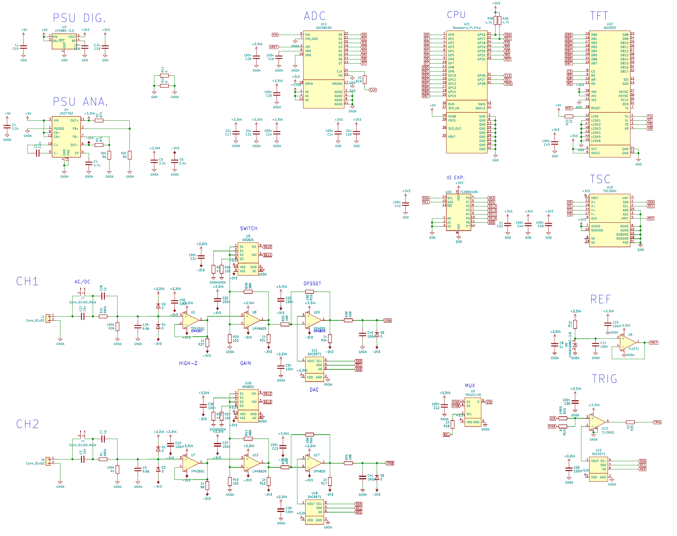
In the general scheme we see the power part at the top left, the two input channels at the bottom left and the digital part at the top right.
Power Supply
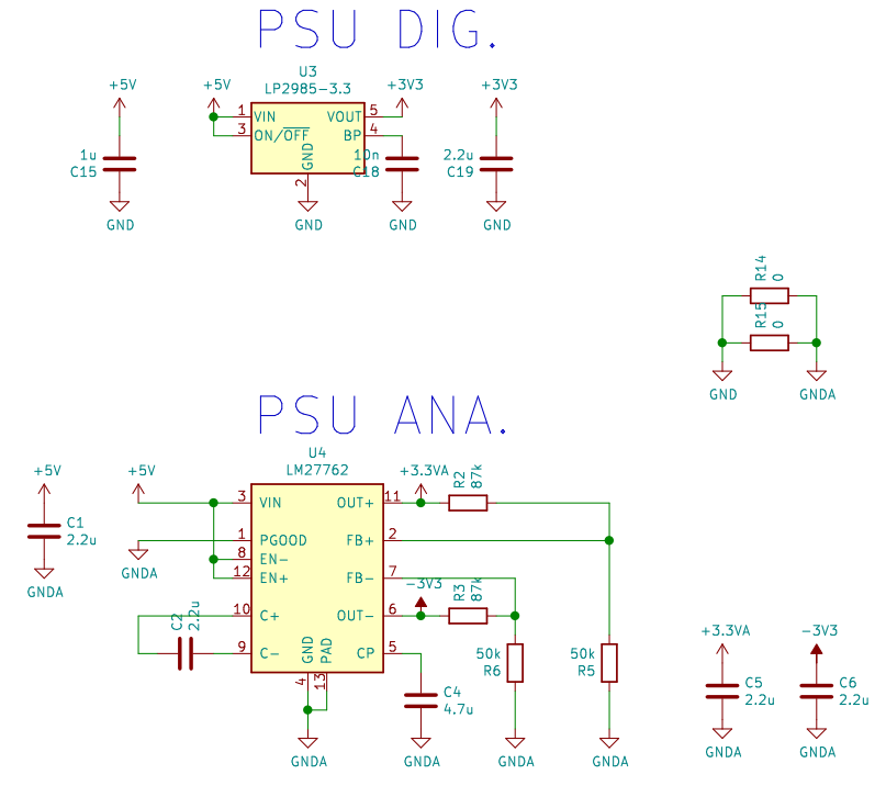
The power supply takes the 5V from the USB and provides 3 voltages:
- 3V3 that will be used for all digital electronics.
- Symmetric 3V3A that will be used for all analog electronics
The integrated LM27762 is a symmetrical regulated source that is capable of generating the negative part using only one capacitor (C2).
CPU block

The main block consists of the ADC, the CPU, and the LCD.
All CPU pins are occupied:
- 8 pins for the ADC bus.
- 3 pins for MUX, ADC and TRIG control.
- 8 pins for the LCD bus.
- 5 pins for LCD control.
- 2 pins for an I2C bus.
- 1 pin for LCD and TSC reset.
Analog front end
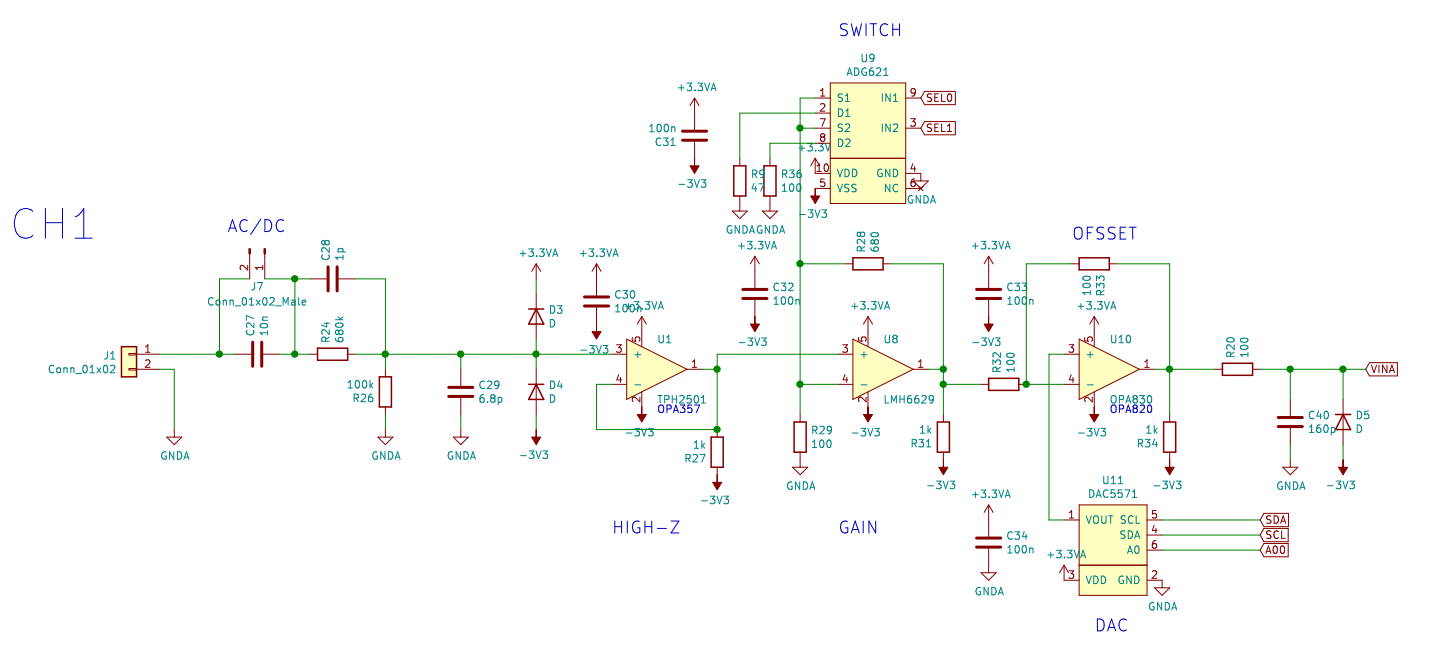
The analog input stage is made up of several passives, 3 opamps, a multiplexer and a DAC.
The input impedance is marked by resistors R24+R26, which is 780 KOhm.
The AC filter (set by C27) has a cutoff frequency of 20 Hz.
The gain of this stage is (100/(680+100)) = 0.12. As the supply of the amplifiers is ±3.3V, this gives us a maximum input voltage of ±27V.

The simulation has been carried out with the Texas Instruments software and all the components have a SPICE model. The bandwidth is greater than 100 MHz and the gain remains constant throughout the entire spectrum.
Analog miscellaneous
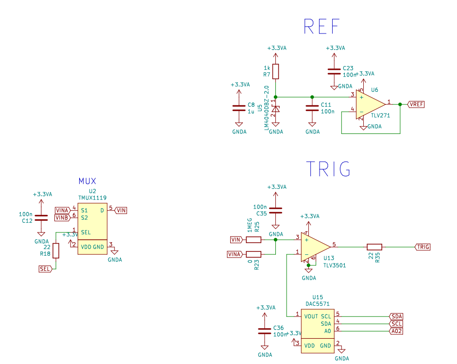
The reference is implemented with a 2.048V zener connected to an opamp configured as an emitter follower.
The trigger is implemented with an 8-bit DAC and a comparator. The TLV3501 is a high speed comparator, with a delay time of 4nS.
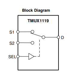
The multiplexer is controlled from the CPU and allows switching from one channel to another. Initially the intention was to do it at 50MHz, but later I verified that these components have a limitation that prevents them from working in this way.
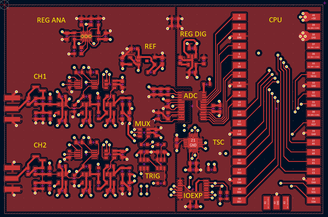
PCB component placing

The components are grouped in clusters with the same functionality and then these clusters are arranged from left to right, starting with analog clusters and ending with digital ones. Also, the power supplies and analog miscellaneous are placed on the upper area of the top layer.
Each cluster is routed on the top layer, connected to the power layers with vias and to other clusters through the bottom layers.
Cluster routing
The analog power supply routing should be as clean as possible. All nets should be as short as possible, specially feedback nets and as wide as possible, specially power nets.
The power input comes from 5V from the upper part and then ±3V3 goes out to the lower part.
Analog PSU routing

The ADC is located between the analog and digital planes. It has the analog part on the left and the digital part on the right.
The analog part is made up of the power pins, the ADC input itself, and the reference. The digital part is made up of the data and control pins.
In the analog part, the routing of the power pins has priority over the signal pins and the latter arrive through the bottom layer.
ADC routing

The front end is the cluster with the most components and is made up of 5 devices. The signal goes from left to right and...
Read more »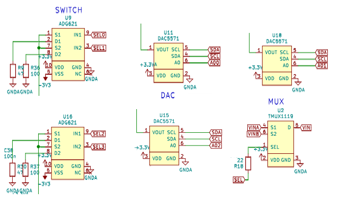


 Emilio P.G. Ficara
 Jithin
 Frédérik Berthiaume
Thank you for the great project, without the schematic I would have been lost.
I built a modified version of this for a university project. It seems though that the firmware in the files is only for v1, so the display is still declared with an i2c connection instead of the 8 bit parallel one realised on the PCB.
Is this something you forgot to upload or is the V2 software still being worked on?