 Joël de Kanter
My goal for this project was to visualise how a IC might be working on the inside. I learned a lot while building this and I hope you can learn something here too. :)
EDIT: Hi it's me from the future. Last semester (2023), as a BcS. EE student, I learned how to desing a digital circuit in a course called "Digitaltechnik". I noticed that a lot of things i decided to do in this project are not entirely against common knowlegde, but also learned some new techniques which i could have benefited from (like karnaugh diagramms).
I also noticed that this project would be very easy to build in a FPGA. Instead of spending 100 hours of designing, testing and building this giant circuit, i could have implemented it in a FPGA in around one afternoon of work. But soldering is also fun! :D
Back to the project!
All details can be found in my written work, but to summarize it shortly (i dont want to write the whole thing in english again hahaha):
UART is a serial communication protocol, used widely in electronics (it is the connection inbetween your Arduino an the USB-bus of your computer, for example).
This is how it works:
Every UART device has a TX and a RX pin. The TX pin transmits data, and the RX pin recieves data.
TX ---> RX
RX <--- TX
So we need 2 wires to connect 2 UART devices (+ Ground).
There is no clk signal wire, so both devices need to agree on the same baud rate (= bit rate or bit/s) which is often 9600 baud.
So for our circuit to work, we need a internal clock generater, but that comes later.
First of all: one UART Message containes

1 Start bit (always LOW) which marks the beginning of a UART message.
5-9 Data Bits (but 8 bits is normally used)
0-1 Parity Bits to perform a parity check, which can detect one (1) flipped bit or fault in the recieved data.
1-2 Stop Bits, to mark the end of the Message
My Configuartion: 1 Start Bit, 8 Data Bits, 1 Parity Bit, 1 Stop Bit = 11 Bit long message.
When there is no information being send over a TX line, then it gets pulled to HIGH by the sender, which is often 5V in the microcontroller world.
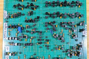
To recieve a UART message, we need to build a circuit called a Shift Register.
My shift register is build from a lot of NAND GATE Latches, which are combined into SRT-Latches and chained together. These are combined into SR-Flipflops. Those can pick bits and move it through the shift register. (EDIT: This is usually done with D-Flipflops, but those require one Transistor more)
A shift register also needs a clock-signal.
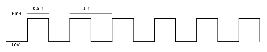
But we cant just slap a clock signal on it al the time. The clock signal activiates all the Flipflops and we want it to start and stop shifting incoming bits exactly when we need it to. Thats why a activation circuit is needed, which lets the clock signal pass through it to the shift register, when there is a UART message incoming. This circuit will also deactivate the clock signals when the message is fully recieved, so it can be stored.
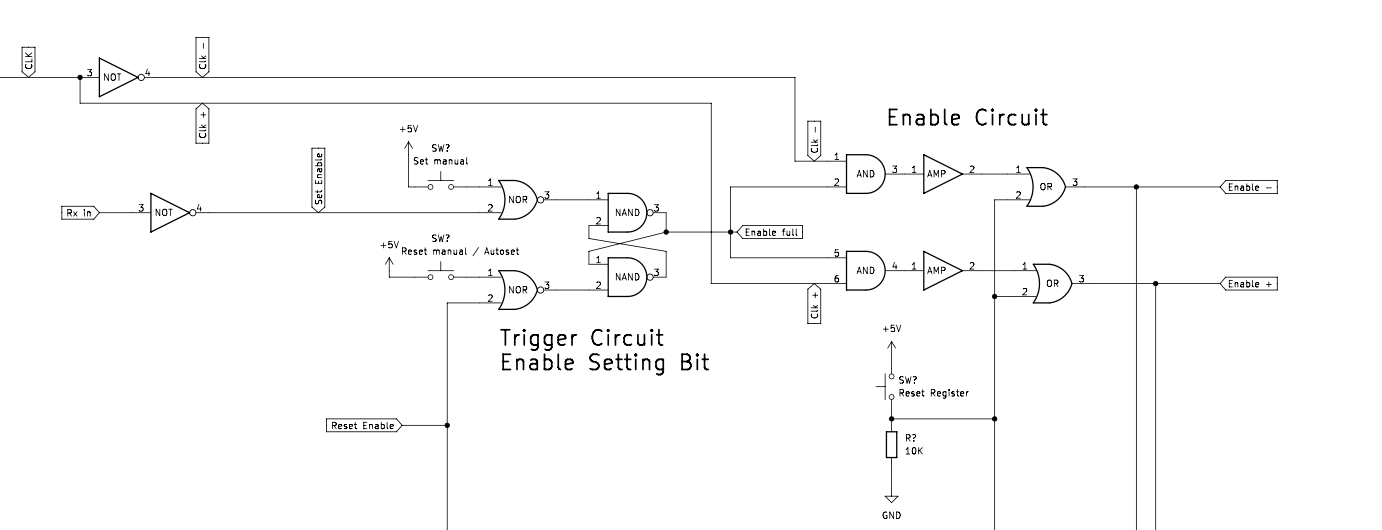
The generated clock signal gets split up in two inverted clock signals (CLK+ and CLK-), which have to pass trough the Enable Circuit to activate the shift register (Enable+ and Enable-). This happens when Enable Full is HIGH, which is controlled by the Trigger Circuit Enable Setting Bit Flipflop (sry for those long names haha). This flipflop can either be manually controlled by two pushbuttons, or, more convenient, is controlled automaticly. When there is a message incoming, the start bit (from the RX IN) will SET this Flipflop, which makes Enable full go HIGH. All the incoming Bits from the RX Line will now be stored and shifted in the shift register, including the start bit. After 10 clock cycles, the start bit (LOW) will have passed through the shift register and will be inverted to a HIGH on the Reset Enable line. this RESETs the Flipflop. At the same time, the Stop bit will be on the RX line, which prevents the Flipflop from SET-ing...
Read more »


 zpekic
 Eric Ljungquist
 Dave Collins
Great project! Quite probably this was exactly the way such circuits were implemented before first UART/ACIA chips appeared in early 1970. Btw, check out my approach to the same problem, which does not use the usual T/2 trigger logic at the start bit: https://hackaday.io/project/181664-intel-hex-files-for-fpgas-no-embedded-cpus/log/197810-ser2par-a-novel-uart-receiver-delay-line-approach