 Vijay
Vijay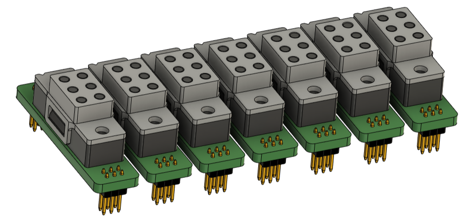
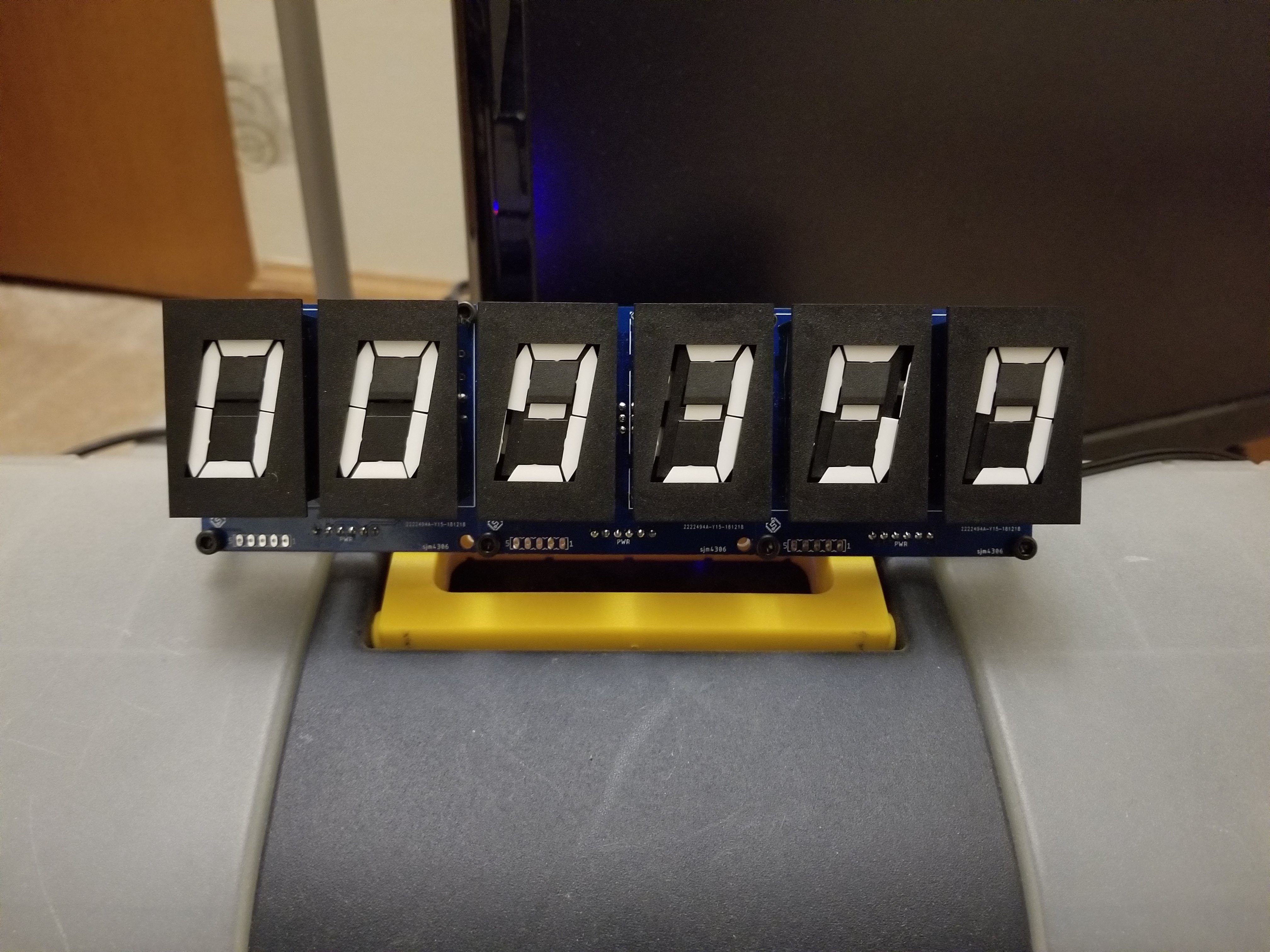
I'm working on the drive electronics to actuate pins for an array of braille cells that can make up a full braille display.
I have been looking into the functioning of Flip-Dots, as they share many similar characteristics to each Braille-Cell dot.
Above: A single Flip dot toggles its position when the polarity of an electromagnet is changed.
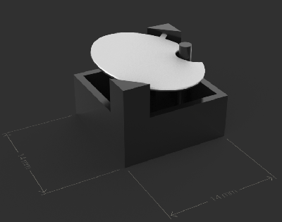
Above: A single Braille dot toggles its position when the polarity of an electromagnet is changed.
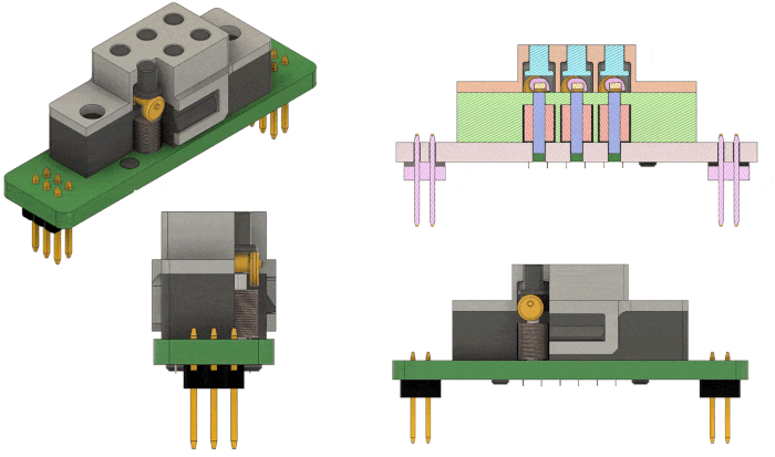
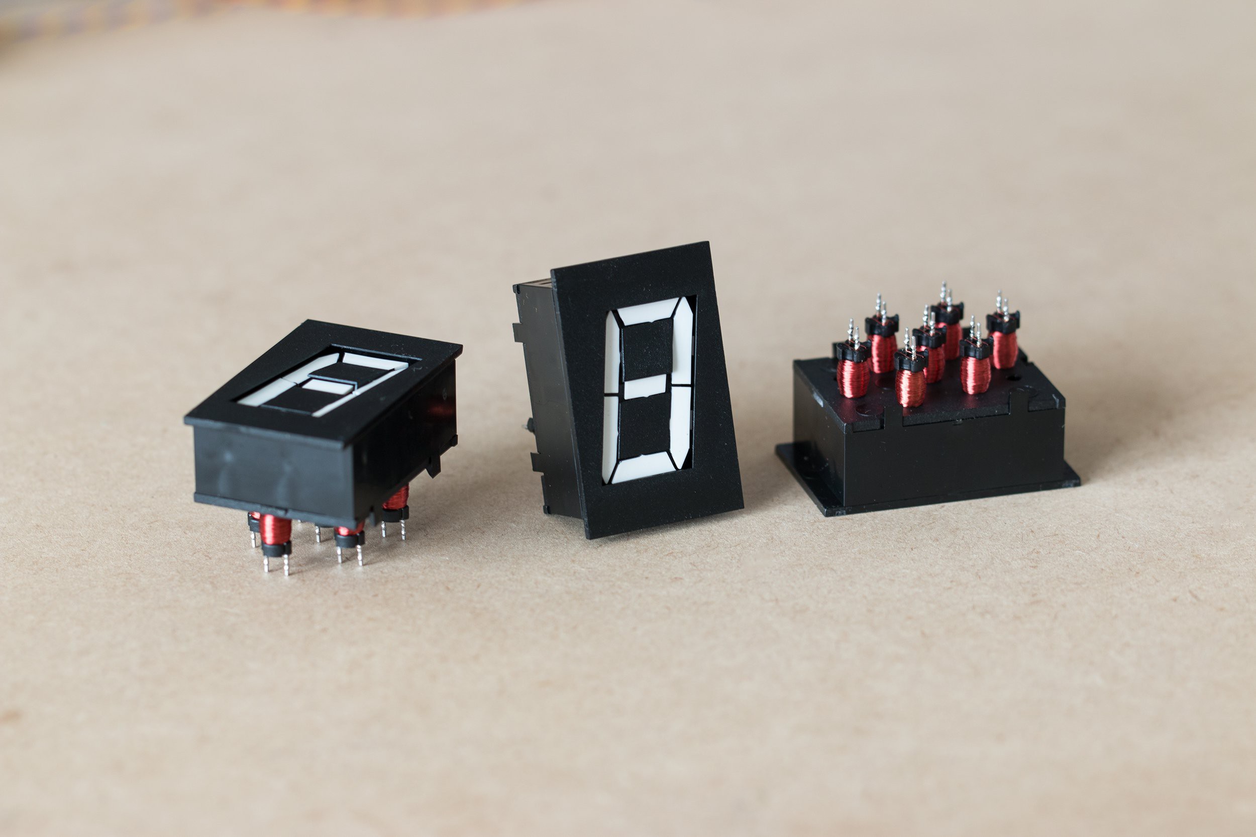
Luckily, there are several projects on Hackaday to learn from (Hackaday community seems to love these). I found these amazing mechanical 7-Segment displays from AlfaZeta that are a perfect analogy for the Braille-Cell, each segment works just like an individual flip dot, and 7 segments of them are packaged into a module where each segment need to be energised only momentarily and then retains its state, similar to our 6-dot Braille Cell:
I found a project that just "Throws H-Bridges" at the module to drive them, but I wanted to be able to save on money and microcontroller pins to create a more elegant solution, and keep the cost lower than the 10$ per Braille-Cell goal I have for the project:
https://hackaday.io/project/162065-wifi-flip-clockyoutube-counter
I came across this video by YouTuber GratScott! that showed an array of these modules controlled by some interesting electronics:
The circuit on this is what Ive decided to reverse engineer as best as possible for a using 6-dot braille cells.

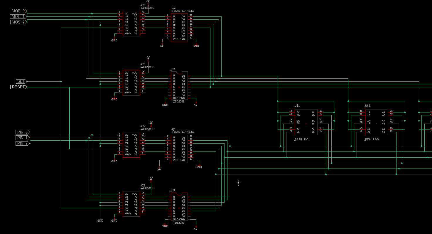
How the driver works (I think), taking the example of driving 5 Braille Cell Modules:
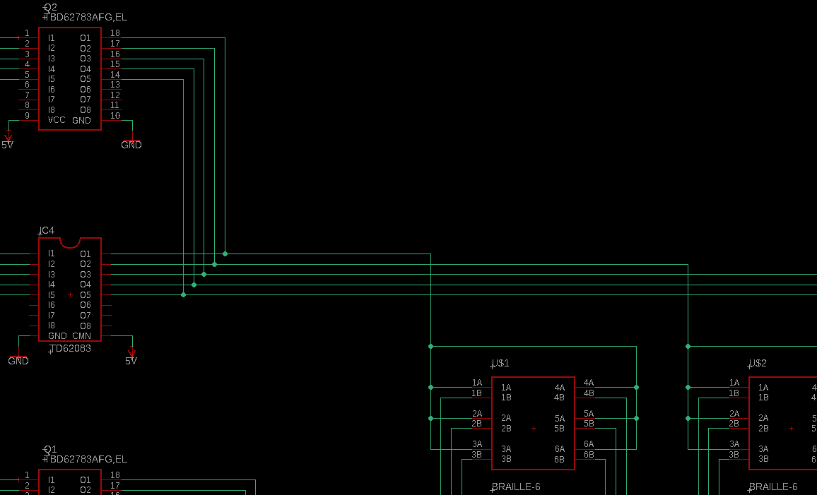
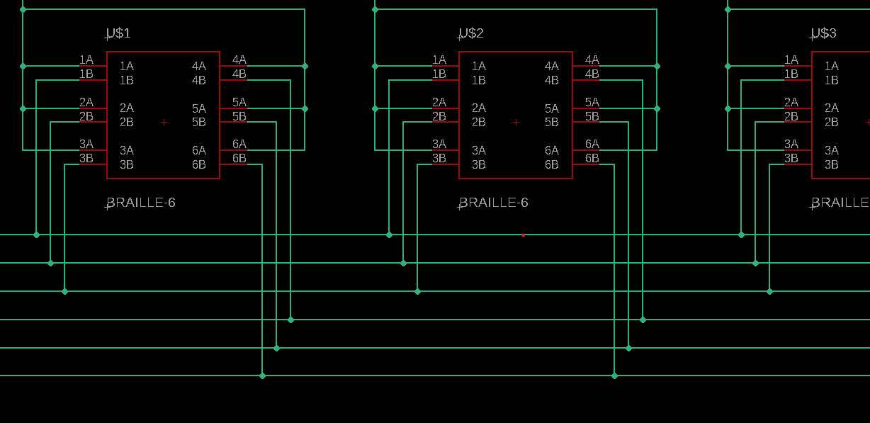
- On each 6-Segment Braille Cell, one end of the solenoid of each segment is connected together in common. Pictured below is the schematic, 1A and 1B are a single coil, 2A and 2B another, and so on. The A's of all coils of a single module are connected together.
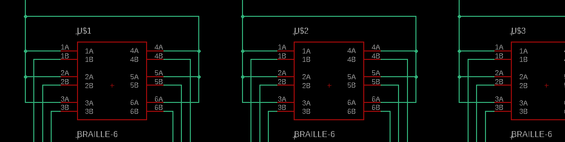
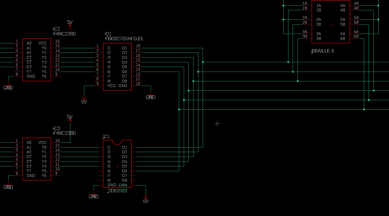
- Each common connection of every Braille Cell is connected to a channel of a source type DMOS transistor array(TBD62783APG https://toshiba.semicon-storage.com/info/TBD62783APG_datasheet_en_20160511.pdf?did=30523&prodName=TBD62783APG) as well as a Sink type transistor array (TBD62083APG https://toshiba.semicon-storage.com/info/TBD62083AFG_datasheet_en_20160511.pdf?did=29893&prodName=TBD62083AFG , Similar to a ULN2003) creating a Half H Bridge circuit
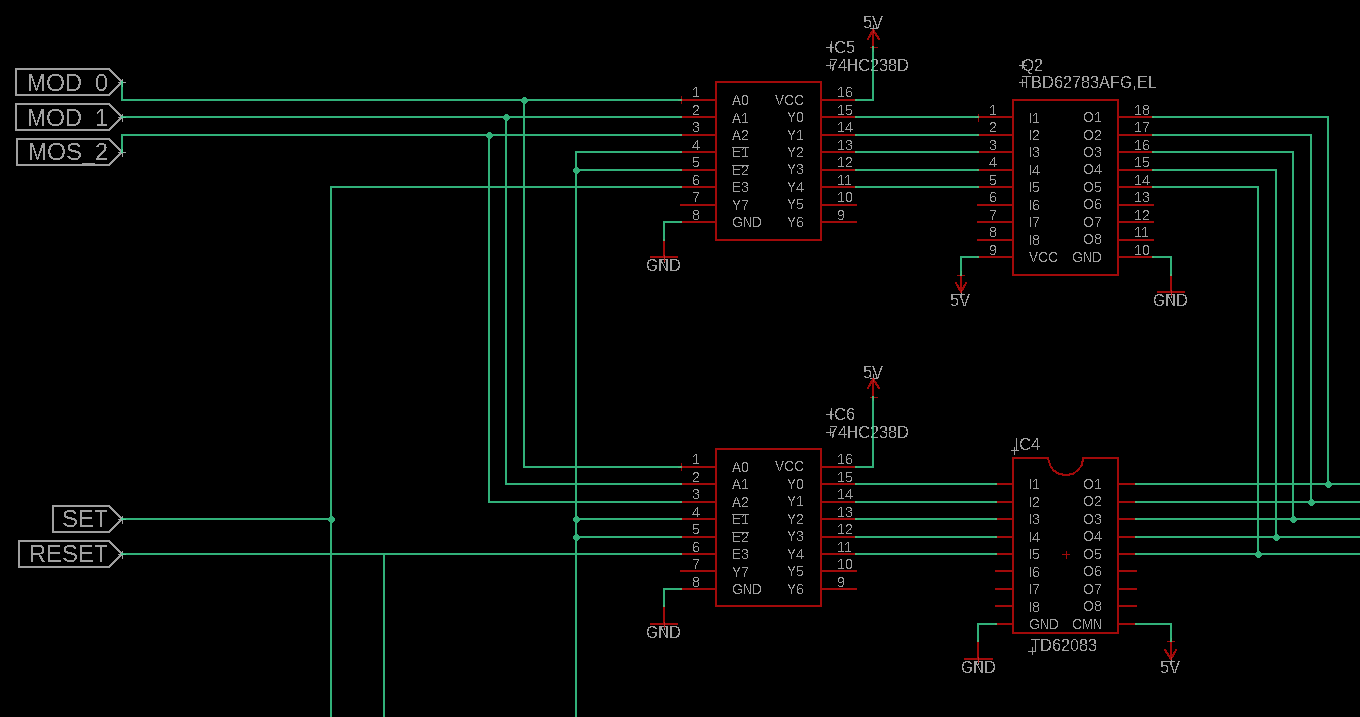
- The inputs of both the source and sink transistor arrays are connected to two CMOS 3-to-8 Decoder ICs( (74HC2238D https://toshiba.semicon-storage.com/info/74HC238D_datasheet_en_20160804.pdf?did=37298&prodName=74HC238D ) . The inputs of both these decoder ICs are connected together to MOD_0, MOD_1, and MOD_2 which will go to the MCU pins. These will be responsible for selecting which module to select for driving.
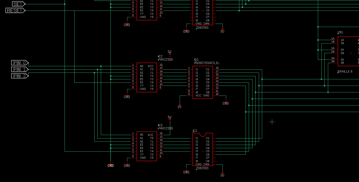
- SET & RESET are connected to the Enable PIns of the decoder connected to the Source Transistor Array and the SInk Transistor array respectively. These will be responsible for connecting the common connection of each Braille Cell Module to the source or sink by activating the decoder-transistor IC pairs. SET and RESET Cannot be both HIGH or else the half H bridge will be in a "shoot-through" state, releasing magic smoke.
![]()
In a similar manner, the other end of each coil of each braille cell is connected in parallel with the respective coils of other braille cell modules.
![]()
These are in turn connected in a similar arrangement as the common connections for each module, connected to a source and sink transistor array, controlled with 3 to 8 decoder ICs
![]()
- The inputs of both these decoder ICs are connected together to PIN_0, PIN_1, and PIN_2 which will go to the MCU pins. These will be responsible for selecting which PIn to drive to select for driving.
- SET & RESET are connected to the Enable PIns of the decoder connected to the Sink Transistor Array and the Source Transistor array respectively. If SET was enabling the Source Transistor Array on the Common connection of the module, on the Pin side, SET would be connected to enable the decoder IC that enables the Sink Transistor Array, thereby completing the H-Bridge connection, with half an H-Bridge connected to the Common PIn, and the other half connected to each individual pin.
- Here is what the circuit looks like all together:
Download the Schematic above here: https://cdn.hackaday.io/files/1911818179487904/Braille%20V1.sch
Functioning:
- Consider all pins/modules to be in a RESET state to start, implying all dots are lowered, and the solenoids haven't been activated.
- MCU selects the Module whose pins to activate by settings MOD_1, MOD_2, and MOD_3.
- MCU Selects the Pin of the Module to activate by setting PIN_1, PIN_2, and PIN_3.
- The MCU will give a HIGH pulse ( long enough for the pins to be actuated/raised) on the SET pin, which activates the Source Transistor Array on the common side of the coil, and the Sink Transistor Array on the pin side, in turn driving the current in one direction in the selected pin.
- Other pins are sequentially activated by setting PIN_1, PIN_2, and PIN_3. and pulsing the SET pin.
- Before setting a module with a new pin arrangement, all the pins will need to be reset to the lower position
- MCU selects the Module whose pins to lowered by settings MOD_1, MOD_2 and MOD_3.
- MCU Selects the PIN of the Module to be lowered by setting PIN_1, PIN_2 and PIN_3.
- The MCU will give a HIGH pulse ( long enough for the pins to be Lowered ) on the RESET pin, which activates the Sink Transistor Array on the common side of the coil, and the Source Transistor Array on the pin side, in turn driving the current in the other direction in the selected pin than before.
- Other pins are sequentially lowered by setting PIN_1, PIN_2, and PIN_3. and pulsing the SET pin.
Questions/Doubts I have:
- Want to confirm that the input pins to the TBD62783APG & TBD62083APG are all active HIGH. I'm confused since usually on a source side Darlington, you need to give a LOW signal to actuate it. But that may not be the case as the equivalent circuit is different:
- Since I'm driving inductive loads Should I add flyback diodes in the circuit ( how and where? ) or rely on the Clamp diodes included in the transistor arrays
- Am I missing anything in the circuit? Is there anything I have not considered? Are components/connections missing to get this work?
- Is there a better way to do this driver circuit?
Download the Schematic above here: https://cdn.hackaday.io/files/1911818179487904/Braille%20V1.sch
Discussions
Become a Hackaday.io Member
Create an account to leave a comment. Already have an account? Log In.
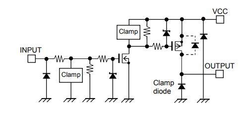
Looking at the TBD62783APG datasheet, it seems that the clamp diodes are specifically added so that inductive loads are driveable.
You might want to consider connecting RESET to !E1 and/or !E2 on the 3-to-8 source decoders (where SET is E3) to prevent the shoot-through condition.
Are you sure? yes | no
Great Idea, prevent any mistakes from happening, thankyou!
I tried simulating the circuit on SPICE, but it would give unpredictable behavior when I connected the Source and Sink array outputs on each of coil side. It works when I test the SET and RESET circuit in isolation, but it seems like you cant just connect these together like in a H-Bridge.
While researching today, I found another project that uses a similar circuit: https://cdn.hackaday.io/files/1594156820411360/Flipdot-Controller-Prototype-v1.pdf
The flip dot circuit it drives has additional components, mostly an array of dual-switching diodes : https://hackaday.io/project/159415-flip-dot-display-diy-controller/log/149305-matrix-layout-and-controllers-job
Adding these into the circuit seems to have got it to work on SPICE, to be seen what happens to it in real life.
Are you sure? yes | no