 Bharbour
Creating a schematic diagram from an existing board can be done. It is somewhat time consuming and accuracy is not perfect, but it can yield a usable schematic to work with an old board. In this project, the board is a VME Bus CPU board using a Motorola 68000 CPU. There is a reasonable amount of DRAM storage and EPROM storage on the board as well as a 2 channel UART for communications. The VME Bus interface is standard, so documentation on that connector is readily available. Data sheets on all of the chips on the board are available. The CPU and all of the programmable parts are socketed, making them easy to remove.
Since I only have one of these boards, destructive methods such as de-populating the board are out. The board is at least 4 layers and may be 6. Holding it up to a light, you can see light through areas that are not covered by components, so there are no ground or power planes in the board.
Before I invested the time required to create the schematic, I wanted some indication that the board was not completely dead. I connected a 5V power supply and ground to the appropriate connector pins and looked for activity on the address and data buses around the EPROMs. There was none. VME boards are designed to be run in a card cage with a backplane board providing power and a number of signals. Thinking that some of the control signals might need to be pulled up or down before the CPU would start, I laid out a PCB with the VME connector, the required resistors and a power connector. When the boards came back from OSHPark, I built one up and repeated the test. Watching the EPROM chip select signals, the processor was performing 4 read operations, attempting to load the reset vector and then halting. The 68K processor will only accept an even value for the reset vector, and if it gets an odd value, it shuts down. The 4 read operations were promising. I dumped the contents of the EPROMs using an EPROM programmer tool and examined the data. The vector table starts at address 0 in the EPROM. All of the addresses in the first 32 bytes were showing 0xFF values. It appeared that most of the other vectors might be sane, but bit rot had trashed the reset vectors. This would explain the 4 read attempts (2 16 bit reads for the stack pointer and 2 16 bit reads for the actual reset vector). Bit rot was not a surprise since the date on the board itself was from 1986, and beyond 10 years EPROM data gets suspicious. Without documentation, creating replacement EPROMs is not possible, but so far it looks functional.
Power supply current on this relatively small board seemed pretty high, at about 1.6 amps. Digging through the data sheets on the parts that seemed to be getting warm, I added up the current draws and the total came out to about 1.6 amps, so that put that issue to rest. I had forgotten how power hungry these old boards were.
In the past, I have reverse engineered a few boards. The method that I used was to use an ohm meter, look for continuity from pin to pin on the IC's, drawing the results on a piece of paper. This method involves constant digging through the data books on the parts to get signal names for each pin.
This time, using my CAD software, I put schematic symbols for all of the parts visible on the board on a few B size sheets of paper. Part placement on the pages was done via best guess and if found to be bad, moved around as I learned more. Part designators on this board are mostly underneath the parts or absent. I hand drew a map of component locations using my own designators that matched the parts on the B size sheets. Working from these sheets, getting the address and data buses penciled in went pretty quickly. Those connections got added into the growing schematic sheets. Mapping the control logic took a lot longer. Using the growing drawings, I could tell where signals were missing and was able to fill most of them in. After numerous iterations, the schematics are about 80% complete. Most of the...
Read more »
 drewrisinger
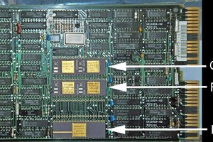
 Pavel
Pavel
Hi Paul, the single probes on my meter are enough. This board is probably the densest through hole board that I have ever seen. More probes would get difficult to manage.
Yes, a fast response beeper is important! Wiping rows of pins is exactly the way I did it.
Thanks,
Bob