 mihai.cuciuc
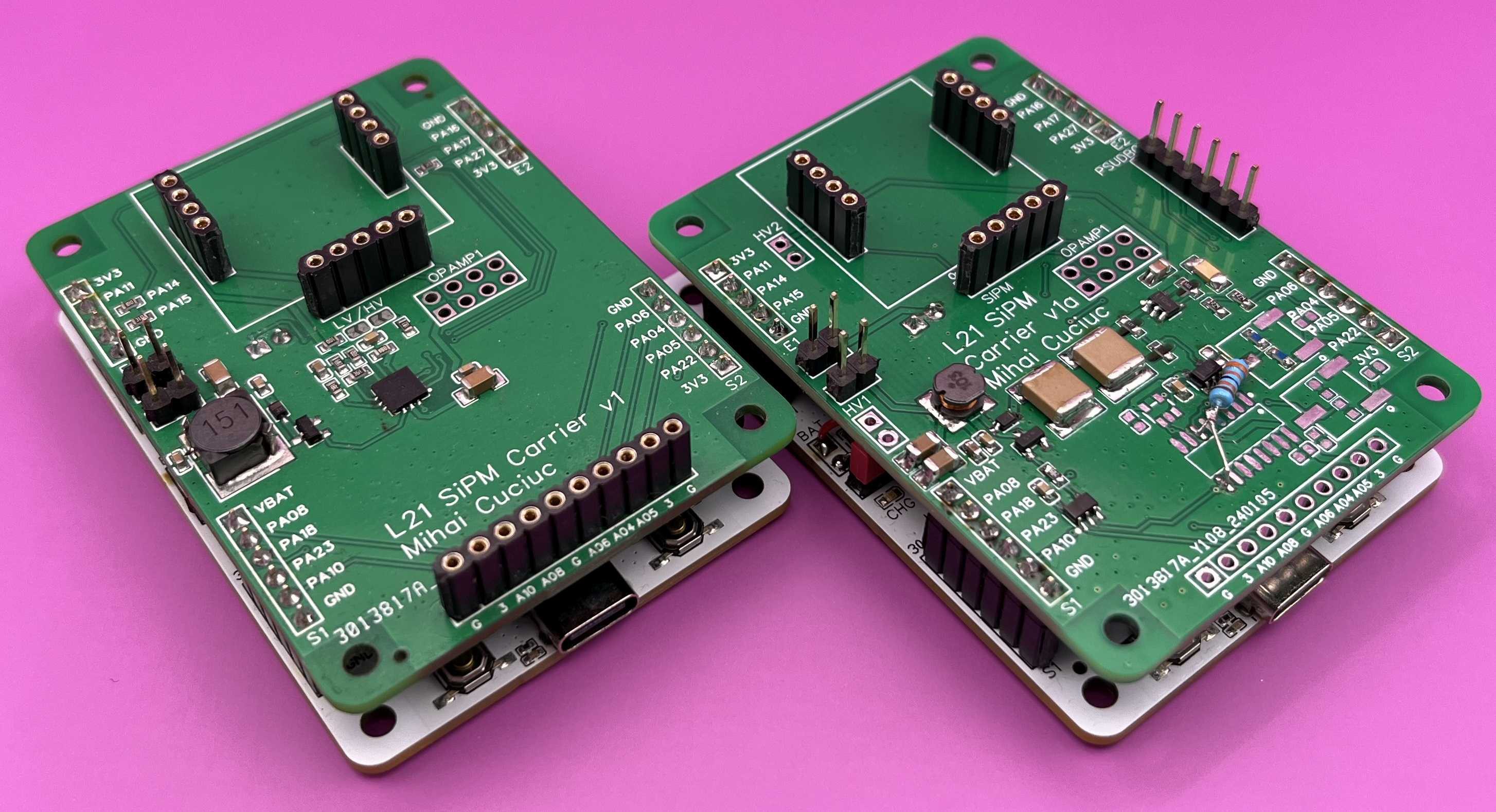
Two PCBs to test different SiPM bias supplies. Left one is MAX1932 board, right one is a lower power version -- but it is a little worse and not as plug-and-play. This log entry describes its design and performances.
The MAX1932 is an excellent chip for biasing SiPMs, but I couldn’t get it to be low power enough for my application. It draws 4.35 mA from the 3.3V line while generating 41V for the SiPM. When switched off, it still draws 0.45 mA. As I’m targeting very low power consumption, I need better, even if I do end up paying with lower performance and increased circuit complexity. I designed a two-stage supply – a boost converter that generates some high voltage with very loose requirements on regulation, followed by a linear regulator that supplies the exact bias voltage needed by the SiPM.
Stage 1 – Boost converter
I was amazed by the performance of the Compact, low-power Geiger counter developed by BleakyTexwith an incredible attention to detail. He is using a custom boost converter to get to ~100V, and then a voltage multiplier to get to the ~400V that his Geiger tube uses. I decided to shamelessly steal his boost converter design, without the voltage multiplier. As I use a linear regulator afterwards, I don’t really care what the output voltage of the boost converter is. It's ok as long as it’s higher than the highest voltage I’ll need, and lower than what would fry the linear regulator. These loose requirements really help lowering the average power draw, as I can let the boost converter run to ~60V and switch it off until the input to the linear regulator drops below ~50V.
I don’t trust my math skills to do a similar analysis to the one BleakyTex did, but I did run a toy simulation in PSpice for TI.
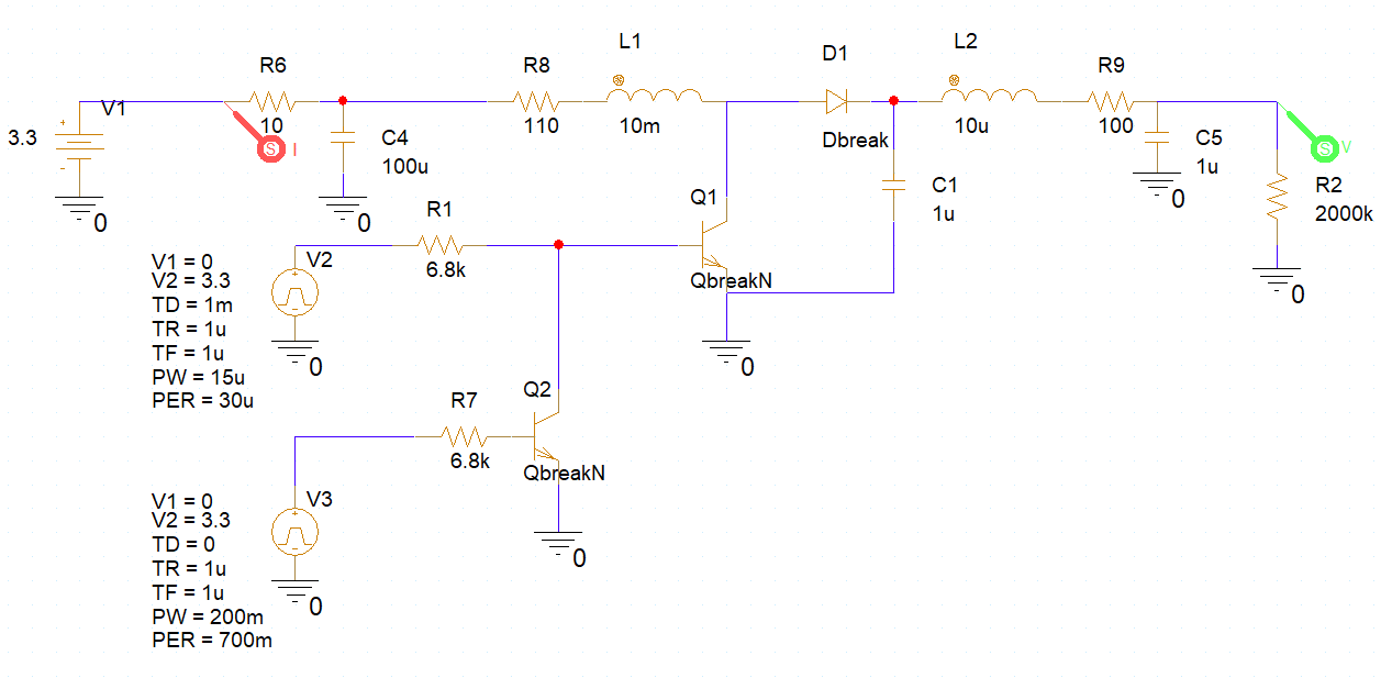
PSPpice for TI simulation schematic for the boost converter. Red probe measures input current, green probe measures the output voltage. R2 is a load to draw ~35 uA, to account for LDO, feedback networks, and SiPM.
In the simulation R6 and C4 form a filter such that I can measure the average current being drawn by the converter. Transistor Q1 does the switching at 33 kHz. To simulate what happens when the converter is running or stopped, Q2 sometimes pulls the base of Q1 to GND, thus stopping the converter.. This happens for 200 ms every 700 ms. L2, R9 and C5 smooth the output.
The simulation results are in the following plot.
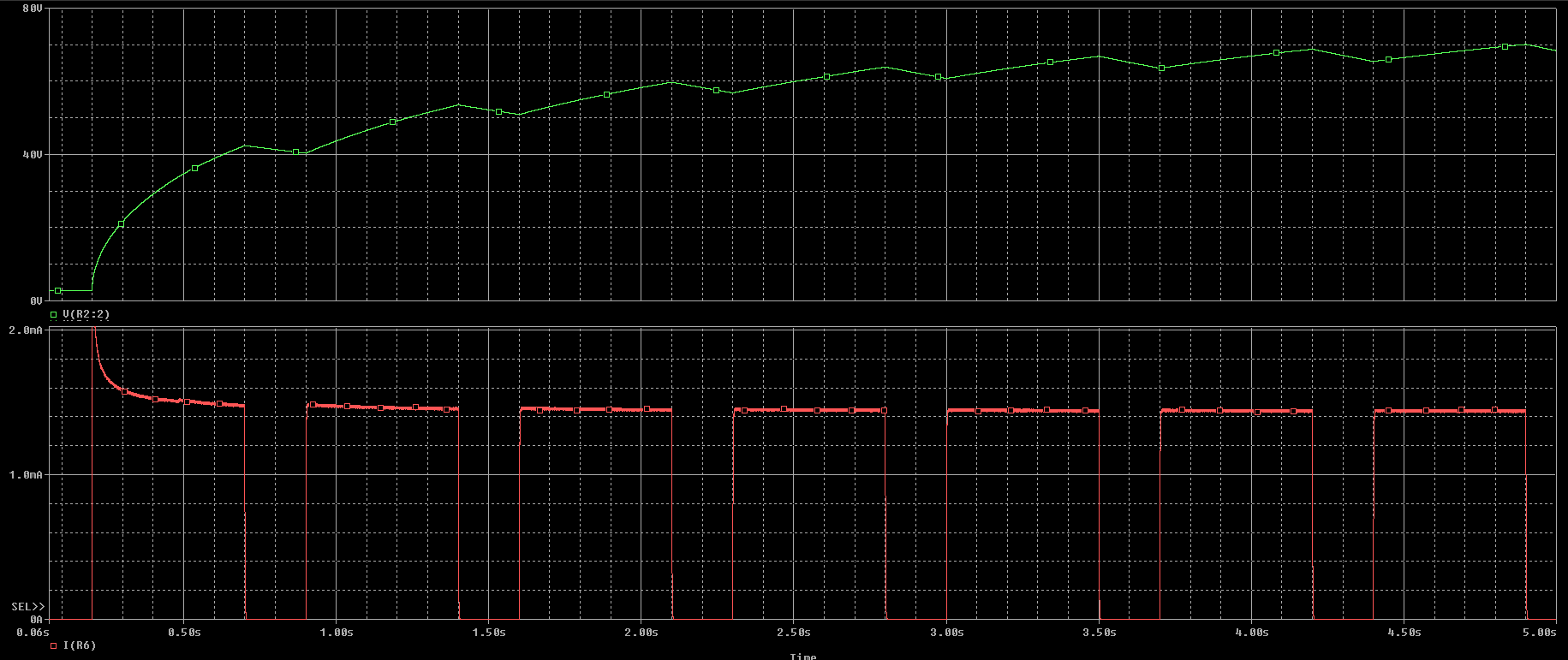
Top green plot is output voltage, steadily increasing over 5 seconds to ~70V. Bottom red plot is current drawn from the 3.3V supply, settling below 1.5 mA when the boost converter is running.
This voltage is fed to a linear regulator to supply the SiPM bias voltage.
Stage 2 – Linear regulator
I chose the LT3014B LDO as it can take up to 80V on its input and draws less than 10 uA. Its output can go as high as 60V which is great because the Broadcom SiPMs I use need somewhere between 32V and 48V. The only problem is that I want to tune the bias voltage on the SiPM from software, and this LDO’s output is fixed by a resistive divider:
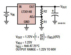
However, if I give the ADJ pin a little nudge with a DAC I can make the feedback loop settle at a different Vout: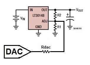
This circuit has Vout = Iadj*R2 + 1.22V*R2/R1 – (Vdac -1.22V)*R2/Rdac. Choosing R1 = 180k, R2 = 5.6M, Rdac = 750k I get:
- Vout = 48V for Vdac = 0V
- Vout = 33.4V for Vdac = 2V
Putting it together
To make the boost converter run I use a 32 kHz output from the MCU, as it runs off an oscillator that has to run all the time anyway for timekeeping. This signal is gated by a comparator that keeps the output voltage within some reasonable limits. Using a single comparator with hysteresis keeps the part count as low as possible. The power supply design ends up looking like this:
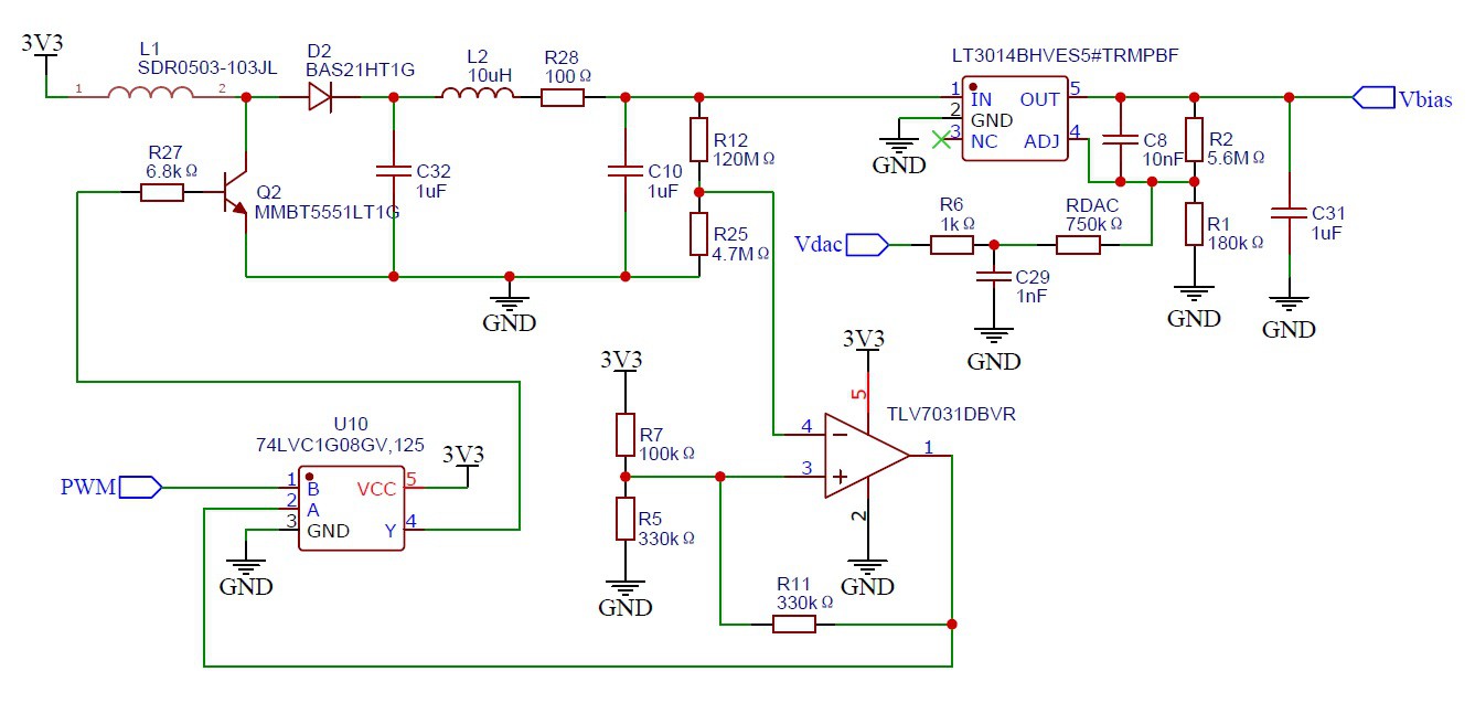
Low power SiPM bias supply. The boost converter requires a 32 kHz square wave input and keeps its output swinging around 50 - 60V. The linear regulator's output voltage can be adjusted by a voltage input at the Vdac node.
The TLV7031 is a very low power comparator. Resistor R11 implements hysteresis to allow the input voltage to swing quite a lot before toggling the comparator output. The 74LVC1G08 is an AND gate that effectively enables or disables the switching regulator based on the voltage at the input of the LT3014B.
In this configuration the MCU retains full control of the bias supply without having to do any housekeeping once it's set up.
A scope picture of the circuit in action shows the boost output, LDO output, and the PWM bursts that feed the switching transistor. The circuit struggles a bit harder than in the “Measurements” section below because of the two prodding 10 Meg scope probes.
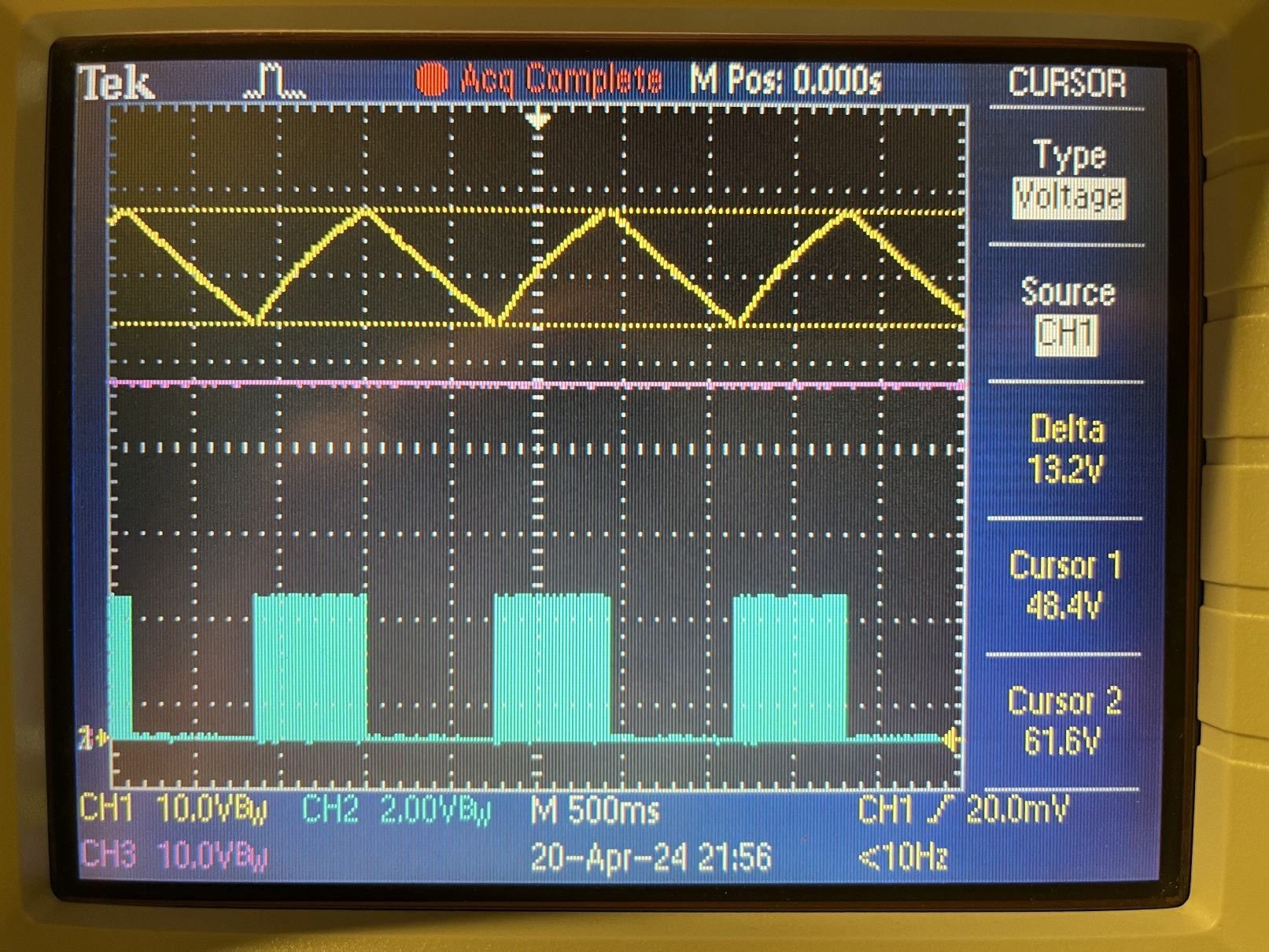
Ch1: Boost regulator output, swinging from 48V to 61V
Ch2: PWM bursts, output of AND gate
Ch3: LDO output sitting at 41V
Measurements
The SiPM bias power supply draws an average of about 600 uA while generating 41V with no load. The average increases to 650 uA with a SiPM connected. This average is the result of the circuit drawing 2.1 mA for about 500 ms while the boost converter is running, and then ~20 uA while it's off. The ~20 uA result from the comparator, resistive divider R7/R5, and AND gate.
These numbers do not include the MCU internals that need to be kept enabled for the supply to run, i.e. 32 kHz square wave generation and DAC. The square wave should be very low power, but I measured two DAC channels drawing ~600 uA. I estimate less than 1.5 mA for the entire circuitry for generating the SiPM bias voltage – much less than the MAX1932. Where my solution does struggle however is with high count rates when the SiPM draws more current. I’ll need to adjust the PWM parameters to increase the current capabilities, but I should be able to do this on the fly, as needed.
Discussions
Become a Hackaday.io Member
Create an account to leave a comment. Already have an account? Log In.