 Keith
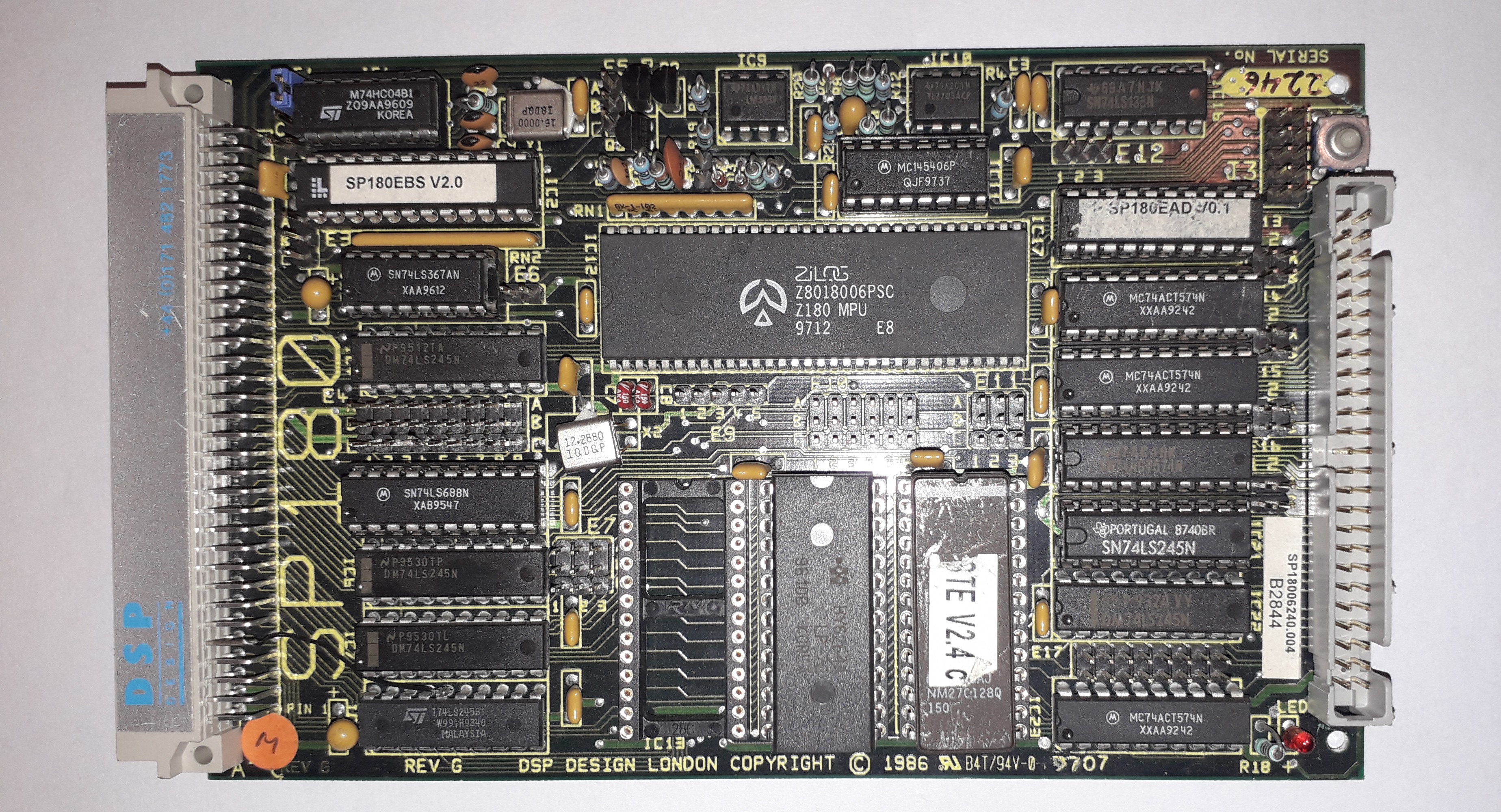
KeithI bought this thinking it was an STEbus master, but in fact it is a slave. It occupies a 4K block of STEbus memory space.
0%
0%
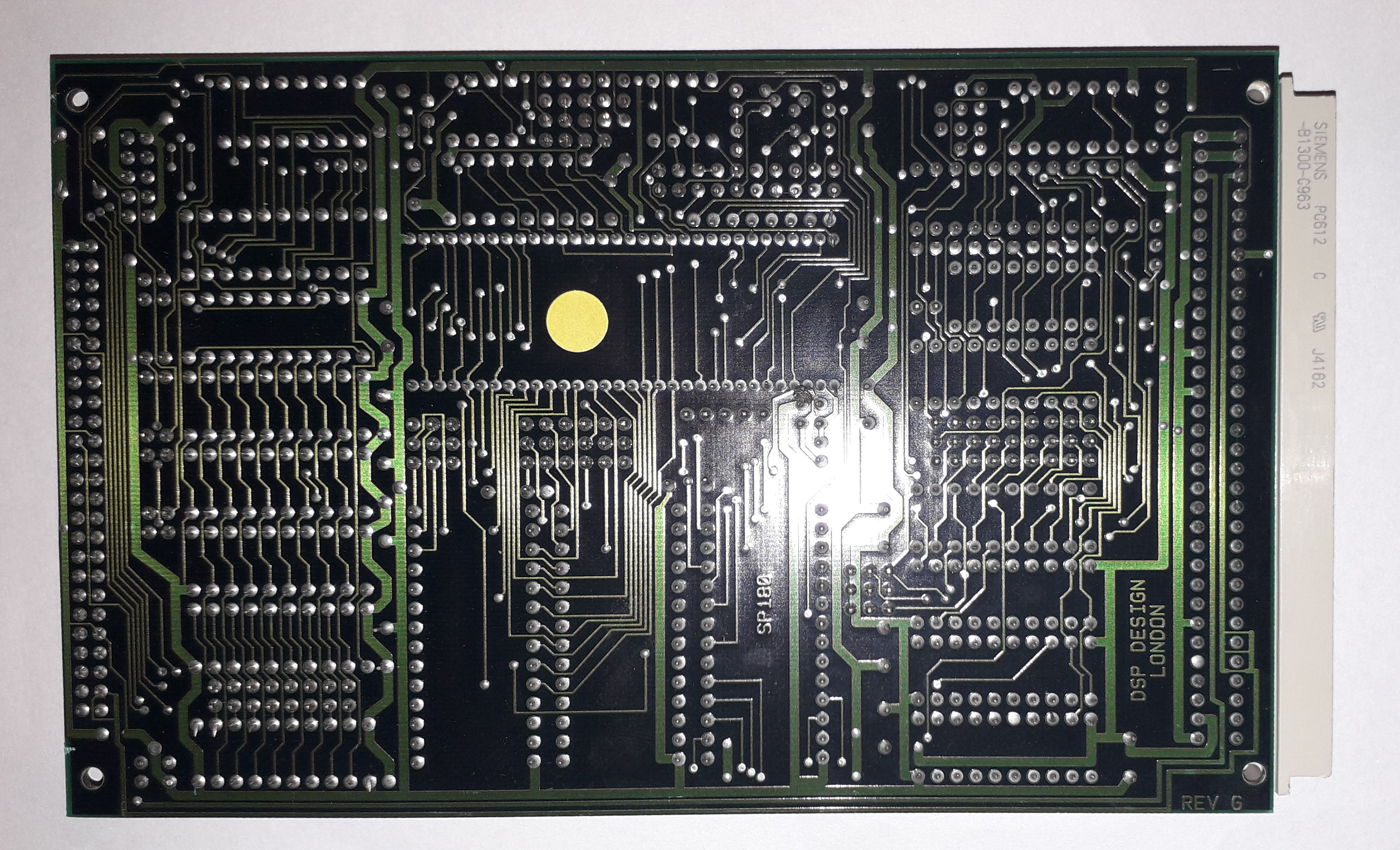
STEbus Z180 slave board (SP180)
The STEbus requests the CPU's bus to access memory space
Become a Hackaday.io member
Already have an account? Log in.
Just one more thing
To make the experience fit your profile, pick a username and tell us what interests you.
Pick an awesome username
hackaday.io/
Your profile's URL: hackaday.io/username. Max 25 alphanumeric characters.
Pick a few interests
Projects that share your interests
People that share your interests
 Craig
Craig
 John Croudy
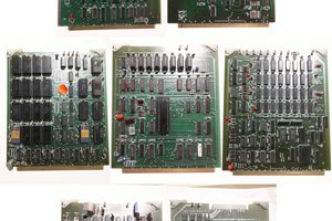
 SHAOS
SHAOS