 sky-guided
Revision 0.3 of the induction driver creates a plasma toroid that's stable and controllable, and does so without overheating.
I'm closing in on a finalized version of the driver. Soon, both the induction coil and driver circuit will be unified into a single monolithic PCB.
This round of prototyping was...
Sponsored by PCBWay!
Entirely to my surprise, a representative from PCBWay contacted me with an offer to cover the costs of a batch of boards.
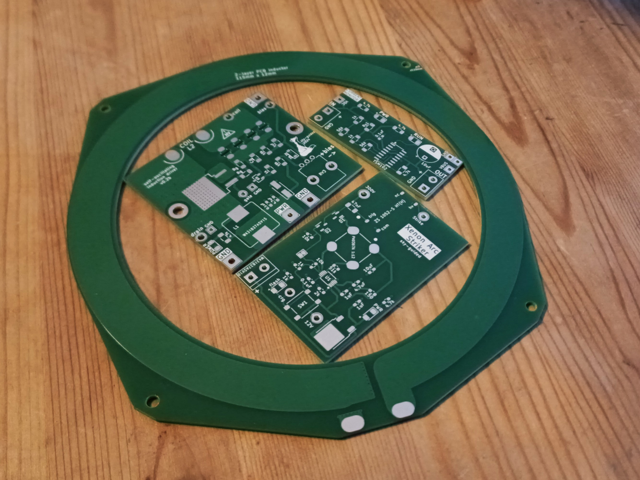
Four boards! Three solder stencils!
(This project log will cover design updates to the induction coil and driver. The other two accessory boards will be featured soon, but there's still a few circuit details I need to refine first.)
Some stuff I like about PCBWay:
- Fast. Eerily fast, sometimes.
- Inexpensive!
- Their instant quote functionality can be super handy for design planning, even before a board layout is finished. For example, it's great to be able to test out possibilities for things like "how much would it cost to make the board 50mm wider? What if I want to use 2-oz thick copper?" Etc.
- Quality is solid. Admittedly I haven't plumbed the depths of BGA or wafer-level-packages yet, but for everything I've done so far I've been totally happy with PCBWay boards.
- If there's something malformed in the manufacturing file, a member of their production team will email asking for clarification of design intent. This has happened to me twice!
- I like they that sponsored me. I'm saying that very sincerely, not just because the monetary windfall is nice (although it really is). It's incredibly endearing that PCBWay is seeking out and financially supporting small, independent projects like this one, and not just big-name makers and youtubers that already attract 100k+ eyeballs.
Assembly
Just like previous versions, solder paste was smeared across the laser-cut stencil, components were placed with tweezers, and the board was reflowed on a budget hot-plate.
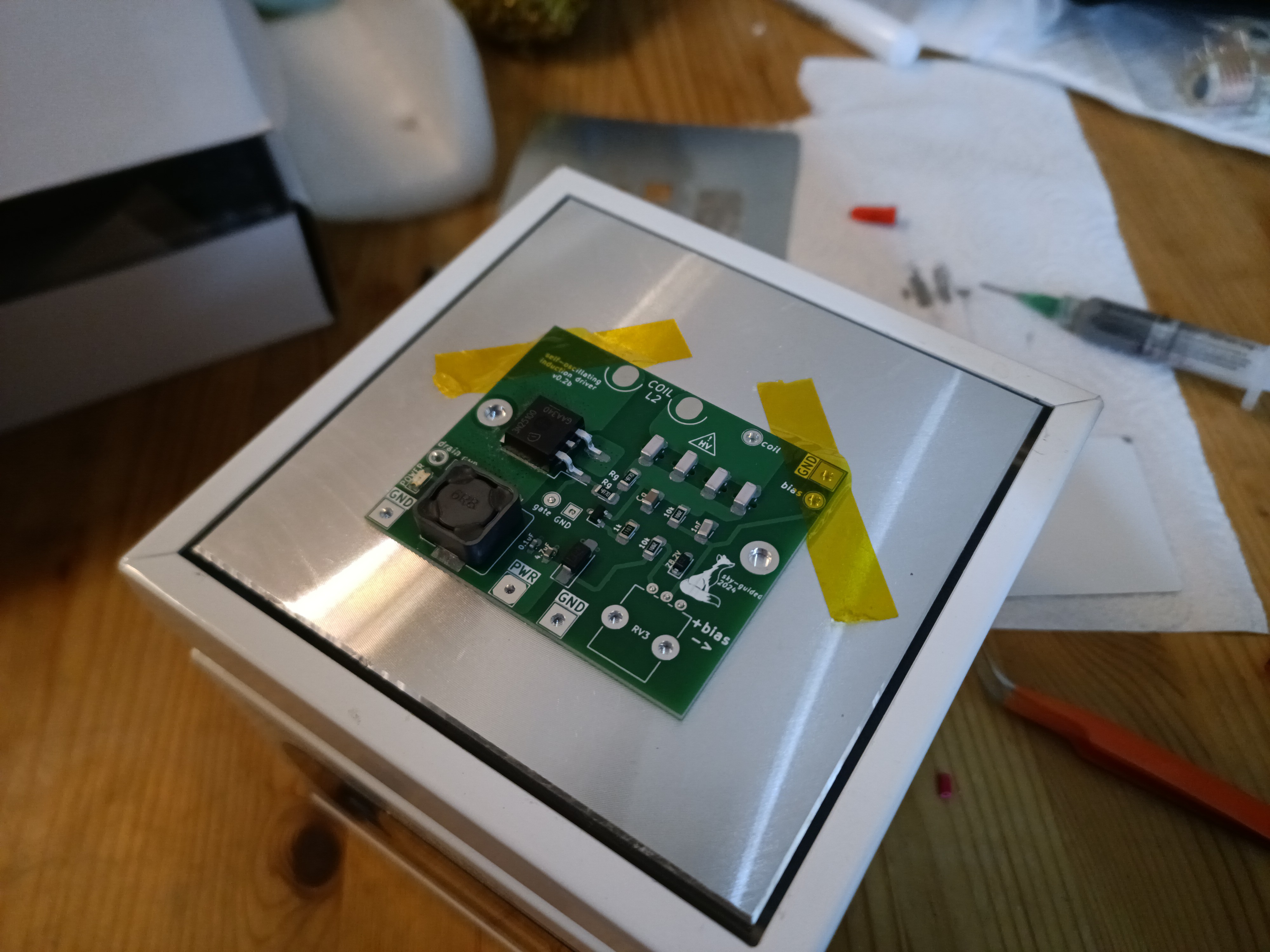
(Kapton tape was used to keep the board in place during assembly, but not during reflow.)
Minor soapbox time: I spent quite a while as an electronics hobbyist being intimidated by surface-mount parts. Secret is, SMD assembly (at least for relatively large components) is faster and easier than strip-board and through-hole. This is especially true with a solder stencil and hotplate (or presumably toaster oven) reflow. Through-hole parts are decidedly obsolescent, and these days most interesting ICs are only available in surface-mount. For this project, using an actual PCB is also hugely important for minimizing parasitic inductances.
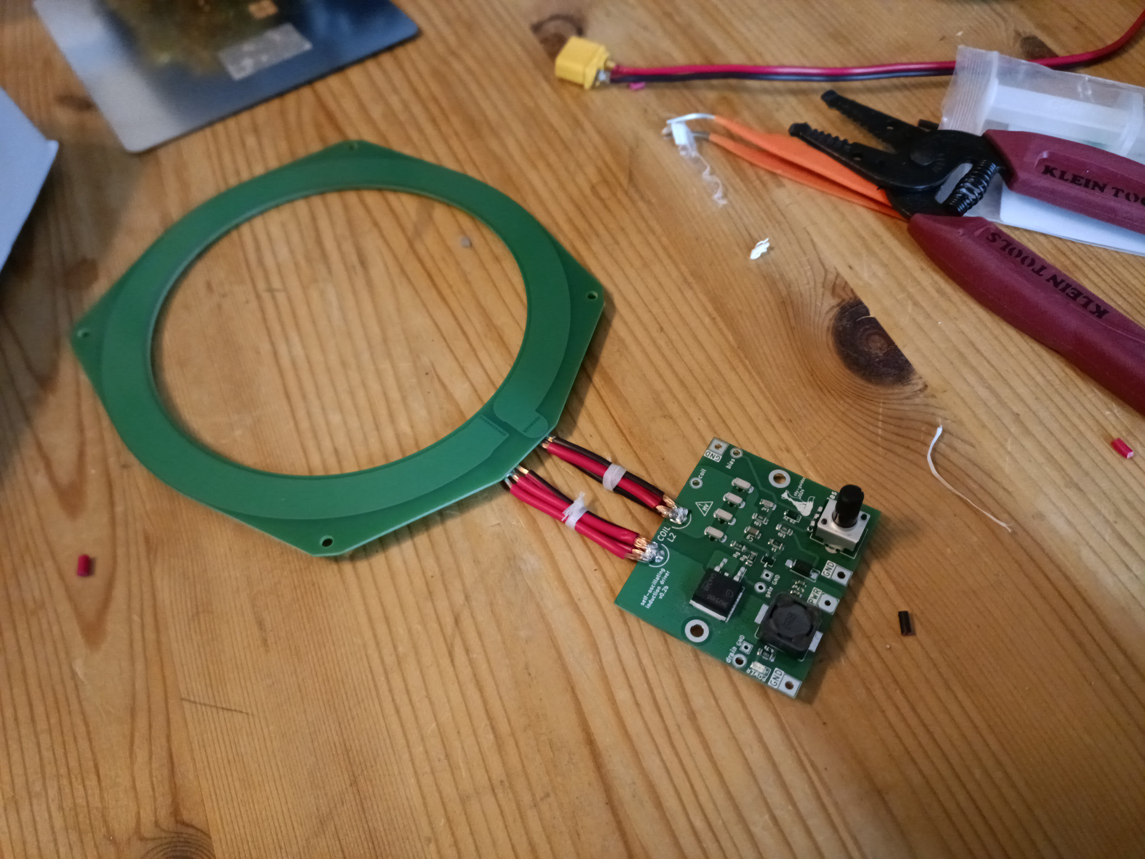
With a larger inductor coil (115mm center-span x 12mm width) and some neater connecting wire bundles, the assembly looks pretty slick!
Here's what changed in driver version 0.3:
No more overkill SiC MOSFET
I'd been considering replacing the Qorvo UJ4C0750 - series SiC mosfet for a bit now. Some of that motivation was due to their cost (at ~$11 each), but performance characteristics drove the change.
I'm now using the Infineon IPB17N25S3-100 "OptiMOS" Si mosfet instead.
For this application there were a few key parameters, at least as I understand them:
Drain-Source voltage: Never seemed to rise above 200V in either simulation or on the bench. Absolutely no need for the 750V-rating of the UJ4C0750. The IPB17N offers 250V, which is plenty.
Drain Current: Needs to be anywhere upwards of 6 amps or so. Again, the new mosfet has plenty of headroom at 17A.
Gate Charge: Without a proper high-current mosfet driver, it seems worthwhile to minimize the amount of charge that needs to be shoved in and out of the gate pin before the device switches. The UJ4C's 37nC is ok, but the IPB17N has a gate charge of only 14nC.
Switching speeds: Longer switching times could result in greater switching losses. Delay and rise/fall times on the IPB17N are as little as a couple of nanoseconds, compared to low tens of nanoseconds for the UJ4.
Output Capacitance (Coss): Steve Ward stresses the importance of C(oss) being fully discharged before switching, and discusses the (possibly substantial) heating due to capacitively stored energy. The UJ4C has a quite low C(oss) value. I almost certainly overemphasized C(oss) as a parameter, which is a big part of what lead to using the UJ4 in the first place.
On-resistance: The UJ4C has an quite low On-resistance of only 58mOhm. It's a bit higher for the IPB17N at 85mOhm, but not that much higher. At the low operating currents of 2-3 amps, it hardly makes a difference.
Basically, parts in the OptiMOS series look super good enough, at about a fifth the price. A lot of the offerings in Infineon's CoolMOS product line also look quite compelling by the numbers, but Steve Ward warns about that SuperFET type device often having unexpected energy losses. I'm increasingly unsure how much I trust that (especially given the CoolMOS datasheets explicitly list C(oss) energy figures that are rather low), but for the moment I'm using the OptiMOS -- and a lot of that decision was fueled by seeing someone else's highly successful build using parts from the OptiMOS series, as I'll discuss in a moment.
Unfortunately, the device footprint of the IPB17N wasn't compatible with the UJ4C, otherwise I'd probably have just bodged other design changes on to the version 0.2 board.
Lesson learned: do not be seduced by new hotness semiconductors unless I have a specific reason to need their characteristics.
The magnificent plasma toroid of Humxn
Recently, a youtube user by the name of Humxn posted a video of their own plasma toroid. Not only is their build cool and clean, they also do a fantastic job of walking through both design details of their (very tidy) circuit, as well as a number of implementation tips and tricks. Humxn also showcases a beautifully stable toroid that can float perfectly in the middle of the xenon globe.
I'm borrowing several design elements directly from them:
- Use of the OptiMOS series mosfet, rather than the CoolMOS I'd been eyeing.
- Using a zener diode to create a voltage reference for the gate bias, rather than just a raw voltage divider from the supply line (which destabilizes if voltage sags due to hitting supply limits). As soon as I saw the zener, I mentally facepalmed at not having considered it sooner.
- Understanding that reduction in driver power helps the toroid float and stabilize. I had assumed that floating was due to high drive power and lots of convection from plasma heating. I'd had it exactly backwards!
- Adding a mm or two of separation between the drive coil and the glass globe (my new inductor revision has a bit of blank space between the inner diameter and the copper trace).
- A greater appreciation for current-control as a way of manipulating toroid behavior.
If you're at all interested in building your own plasma toroid machine, the Humxn video is absolutely essential.
Testing Results
Video is at the top of this log :)
Here's the scope traces with the xenon going full donut.
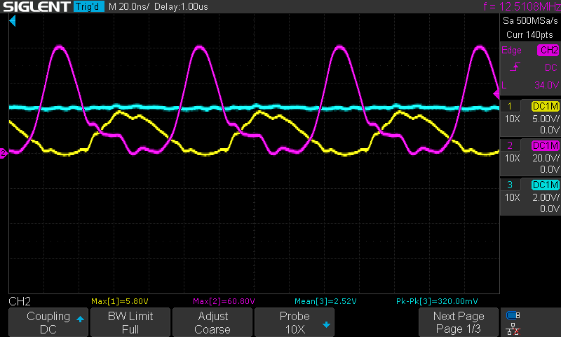 As previously, the yellow trace is gate, purple is drain, and blue is gate bias (note the different y-axis scale). Those waveforms look basically ideal (and I think some of the remaining wigglyness on the drain is due to mediocre scope probing, since I only have so many hands to use pokey leads and not clips). The shape on the drain trace does morph a bit in response to changing drain voltages.
The L1 input choke inductor value was increased to 6.8uH. The previous 2.2uH inductor had been chosen low in an attempt to constrain circuit power draw, but tbh I really should have just planned on setting limits on the supply side.
Adding a 1nF rf-bypass capacitor to the bias voltage network does indeed smooth out that waveform. (Also, turns out I had once again been seeing spurious wigglyness due to an over-large loop area with the ground clip.) Replacing the bias voltage divider with a zener reference also makes striking the toroid quite a bit more stable and reliable. I'm currently using an 8.2V zener but will swap it down to 4.7V soon, to make better use of the full potentiometer range.
I'm realizing that everything I said previously about the using a bias smoothing cap and increasing the impedance between bias and gate-drive causing "runaway oscillation" was total nonsense. Upon further testing, it now seems like the Miniware PSU just dealt poorly with rapid changes in current demand if the circuit ramped to full oscillating power too quickly. This was easily fixed by adding more bulk capacitance at the circuit's supply hookup.
Thermals
Manageable! Running the stabilized toroid at 25-30 watts, the hottest part of the whole project is the globe glass.
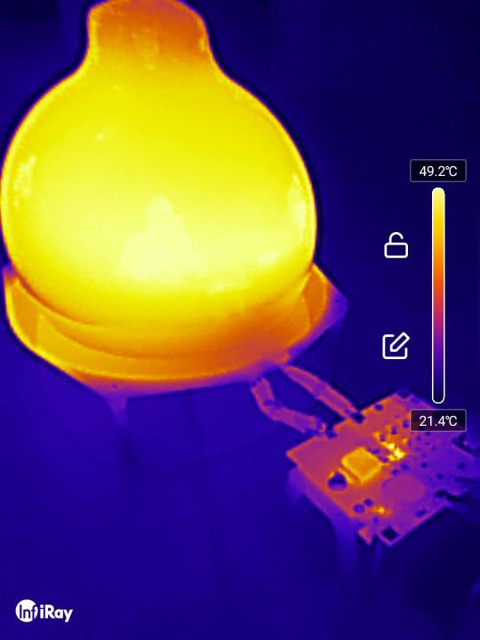
Increasing the trace width of the PCB inductor has helped a lot -- temperatures stayed <50C, or even cooler when the toroid was running at low power.
Performance of the new mosfet is similar to the previous driver iterations. At low power, temperatures (measured infrared at device body) are <60C. Running at full 60-watt power the mosfet still gets probably too hot; 120-130C. I may end up using two mosfets in parallel in the final version. It's definitely not ideal to run at full power for very long (and it seems to offer very little visual benefit anyway), but tightening the envelop of maximum supplied amperage does seem to make the arc start a bit less reliable, when hitting the regulation limit causes the supply voltage to be lowered.
The under-board heatsink has also been mounted and re-mounted several times now, and it's possible that its thermal interface layer isn't making very good contact.
There's a teeny hot-spot on the gate drive resistor. I'll plan on two parallel 1206-size resistors for the next version.
When the toroid isn't ionized, there's quite a bit of heat buildup on the high-voltage side of the (now) four-capacitor primary bank. It's hard to tell for sure, but I think the copper itself is getting hot rather than the capacitors (especially since the gate side of the cap bank stays cool). I'm wondering if parallel-plate capacitive coupling to the ground plane might be causing dielectric losses in the fiberglass? I genuinely don't know if that conjecture makes any kind of sense -- please let me know if that's totally implausible.
Here's my favorite photo from this project so far:
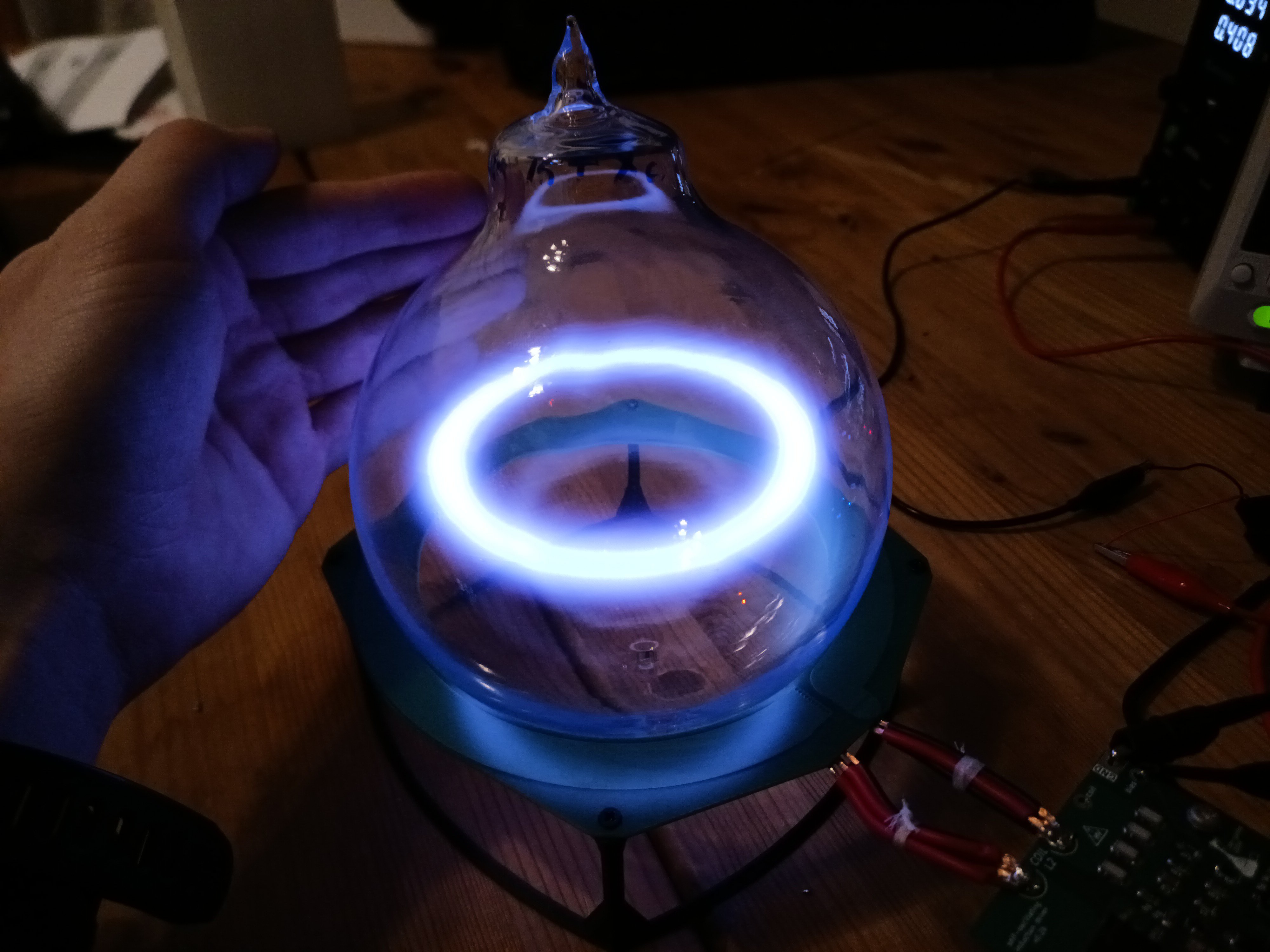
When the toroid is stabilized it looks, honestly, unreal. A little ring of light that floats perfectly centered, still and silent. The dynamic range of the camera can't quite keep up with the plasma's brightness -- IRL it looks more nebulous, more ghostly. (It also plays havoc on camera auto-focus.)
NEXT STEPS:
A key design goal is running the toroid standalone off of USB-C. To that end, I'm implementing built-in power monitoring to indicate whether or not the circuit is in oscillation, rather than needing to read PSU loads or oscilloscope waveforms.
I also very much want to have push-button start for the plasma ionization, rather than the (kinda crude) method of twist-rubbing the globe against the coil.
Unfortunately, neither of those features is working quite yet.
Stay tuned.
Discussions
Become a Hackaday.io Member
Create an account to leave a comment. Already have an account? Log In.
Have you seen the toroid by Humxn..
https://youtu.be/YjTv-Hj0h18?si=a5FyBgSM-hgxyPXE
Are you sure? yes | no
It's literally a section title in this log.
Are you sure? yes | no
I missed that... Lol...I was so focused on your build...
Are you sure? yes | no
I am looking forward to the final version and would like to ask if you can open source the entire project?
Are you sure? yes | no
Full circuit diagrams and general BoM at a bare minimum. *Probably* KiCAD files but I need to think about library packaging (and this revision in particular I did heinous file management, which is why there's no diagram). Native source CAD files for printing would be a privacy challenge (for complicated reasons) but the STEP and/or STLs should be fine.
Are you sure? yes | no