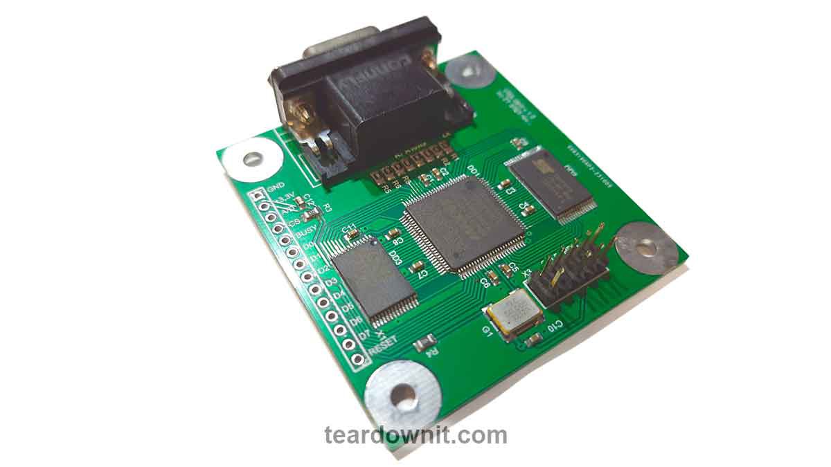
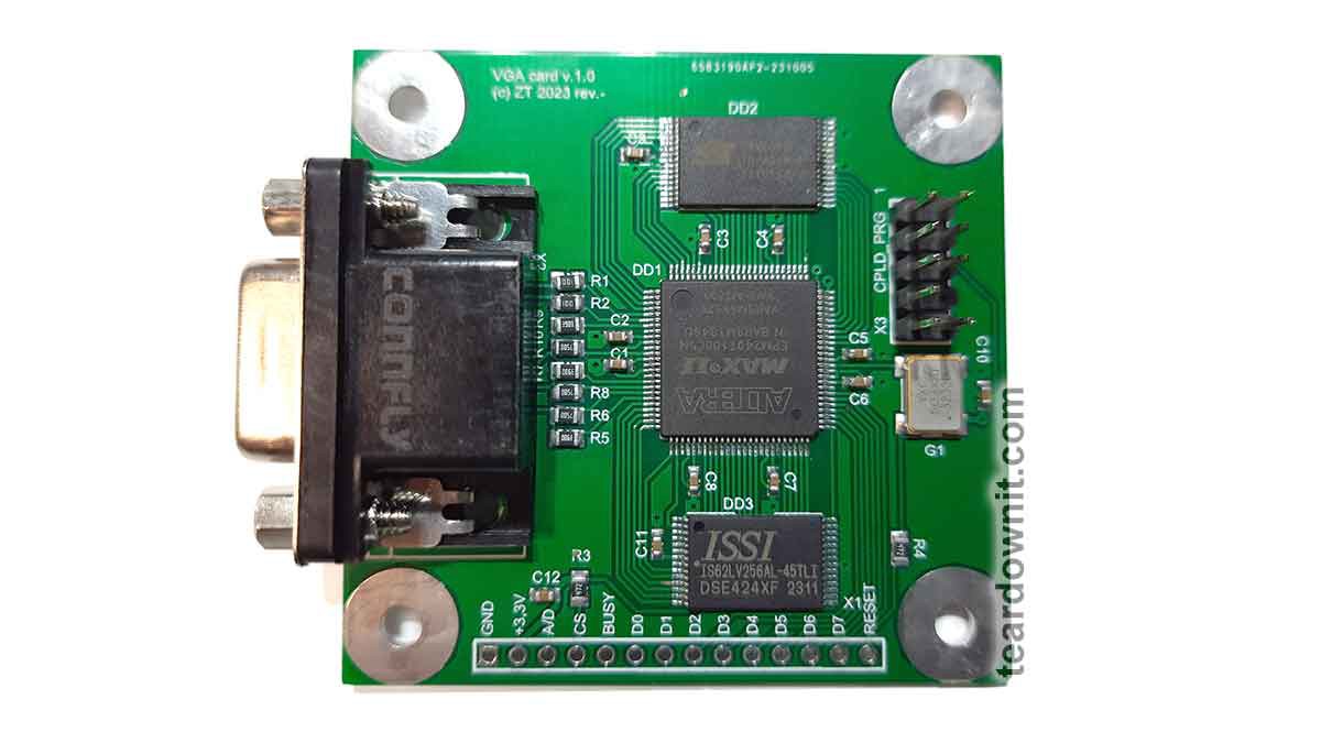
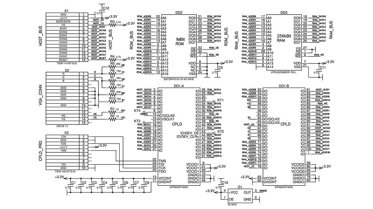
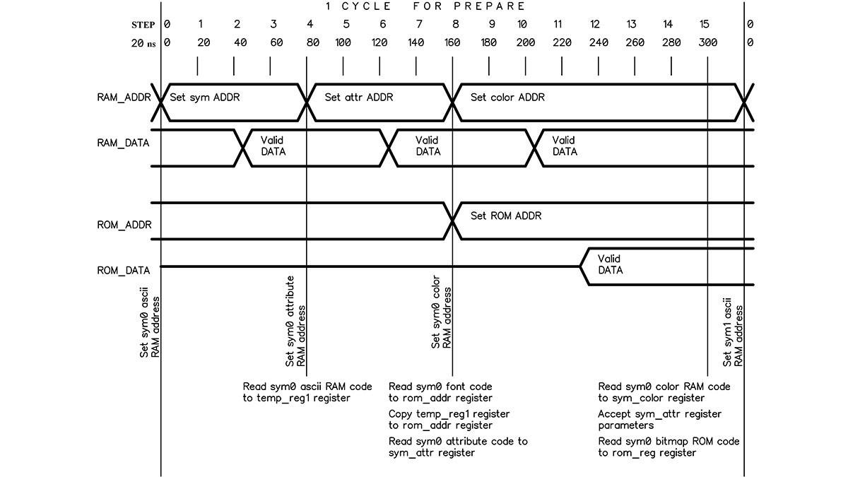
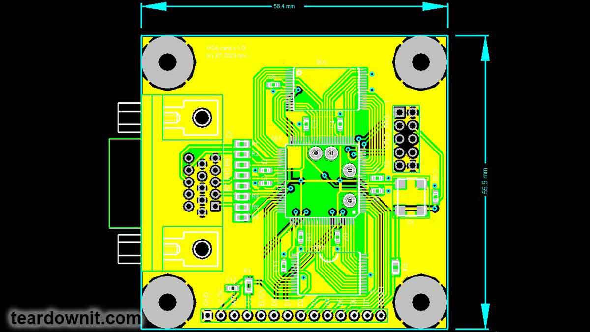
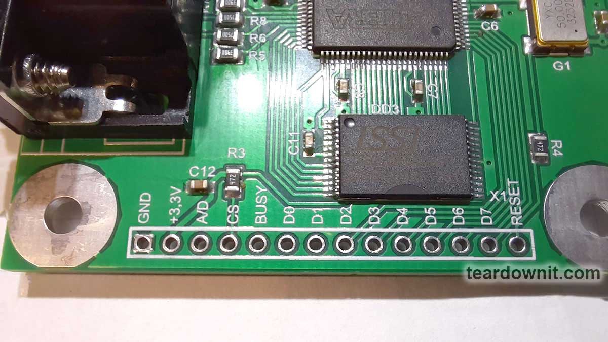
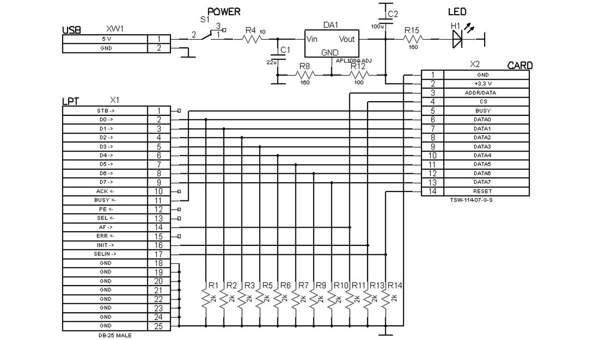
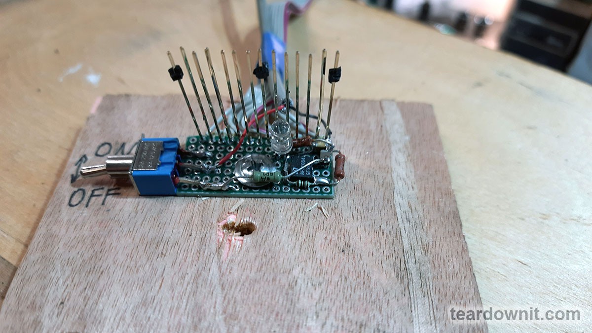
• From prototype to product creation

    teardownit03/13/2024 at 02:17 0 comments

    First of all, you should pay attention to the ROM used. The flash-ROM chip from an old computer motherboard has a finicky parallel interface where the address is written in two runs. This complicates the operating logic and increases access time. Additionally, the PLCC housing it comes in can be expensive and challenging to install manually. In this regard, it was decided to replace it with a more modern 39-series microchip from SST. These chips, such as the SST39LF and SST39VF, have faster access times (55 ns and 70 ns, respectively) compared to 270 ns for the 49 series chip. This allows one to reduce data preparation time to one cycle. The SST39VF010-70-4C-WHE chip has been ordered.

    It is also necessary to replace the RAM. To save money, I picked one that operates precisely at 3.3 V and has TSOP housing. The IS62LV256AL-45TLI chip was ordered.

    The CPLD chip remains unchanged.

    These updates improve overall efficiency by reducing memory access times and using more convenient and modern components, which can also improve product availability and reliability in the future.

    The updated diagram is shown below:

    The timing diagram for new chips has become much more straightforward:

    After the final selection of the main components, a printed circuit board, which had specific requirements, was created. The board had to be adapted for manual assembly. Due to this, components were placed on one side of the board, and the number of pinout components was minimized, leaving only external connectors.

    50 copies of printed circuit boards were ordered. This introduces the risk of the first boards' errors and inaccuracies, leading to scrapping all fifty and re-ordering the whole batch. Also, along with the boards, a stencil for applying solder paste was ordered. This will simplify the assembly process.

    While waiting for the boards to be manufactured and delivered, it was time to think about flashing and testing the finished boards. Flashing CPLD was less difficult and could be done using a separate connector and USB programmer. However, programming the character ROM seemed more questionable. On a development board, to reprogram the firmware, the chip had to be carefully removed from the breadboard panel, inserted into the programmer, erased, flashed, removed, and returned to the breadboard panel. These operations turned out to be quite labor-intensive.
    Therefore, to program the character ROM, it was decided to use the tools of the CPLD itself through a custom parallel interface. There were two possible implementation options:

    1. ROM programming with special firmware installed in the CPLD, intended exclusively for ROM programming.
    2. Implementation of ROM programming functionality into the working CPLD firmware.

    The second option was more complex and required additional CPLD resources that would only be used once or twice in the device's lifetime. Fortunately, there were enough CPLD resources available to implement the second option.

    The finished prototype was tested through the same parallel user interface, displaying the test picture on the screen. To do this, I utilized an old laptop with an LPT port, which provided enough I/O lines to transmit all the necessary signals to the device.

    The testing device (diagram above) was assembled on a breadboard using the surface-mounting method. The resistors were installed in the housing of the DSUB25 connector, and the tested or programmed board was connected with long and flexible pins.

    When bending, the contacts create tension in the board hole, ensuring reliable contact. 2 kOhm resistors, together with pull-up resistors of the LPT interface (approximately 1 kOhm), form a voltage divider. This divider converts the 5V logic levels of the LPT port to 3.3V ones.

    The board is powered through a simple linear stabilizer, getting a voltage of 5 V from the laptop’s USB connector. Resistor R4 with a resistance of 10 ohms is used for current protection. Suppose a short circuit or other problems...

    Read more »

  • Prerequisites and software

    teardownit03/07/2024 at 15:05 0 comments

    Sometimes, when making your own devices on microcontrollers, there is a need to display huge amounts of information on a display and to use a bigger screen for ease of perception. Unfortunately, there are no ready-made and budget-friendly solutions for this task on the market. LCD displays with the ability to connect to a microcontroller are usually tiny and pricy.

    But at the same time, there is a wide selection of legacy LCD monitors with a VGA interface. Models with a diagonal of 15 to 19 inches can be purchased in perfect working condition for a very low price, or one can even get one for free. This especially applies to monitors with a 4:3 aspect ratio. In addition, such models are usually quite reliable.

    Most older monitors only have a VGA connector for connecting to a computer. Sometimes there is an additional DVI port (on more expensive models). The HDMI connector is more common on modern devices.

    Thus, with a probability close to 100%, we'll get just a VGA on an older monitor. In order to display an image on such a monitor, it is enough to work with only five signals: analog R (red), G (green), and B (blue), responsible for the brightness of each color component, as well as digital HS (horizontal sync) and VS (vertical sync), providing synchronization. Analogue signal levels should range from 0 to 0.7 V, where 0 V corresponds to no light at all and 0.7 V to maximum brightness. Digital signals HS and VS are short pulses with a TTL level of negative polarity. The timings of these signals can be found, for example, here: http://tinyvga.com/vga-timing/640x480@60Hz.

    Typically, special controllers, or FPGAs, are used to generate video signals, and many FPGA development boards are already equipped with a VGA connector. However, FPGAs are often expensive and require many additional components. I was looking for a simpler and cheaper solution. As a result, the decision was made to use CPLD. CPLDs have fewer available logic gates (LEs) than FPGAs but are less expensive. For example, the MAX II Altera EPM240 development board is sold on Aliexpress: https://www.aliexpress.us/item/3256804686276488.html for only $8.12 (excluding shipping), and the kit even includes a programmer. The chips themselves can be purchased for $1.6–2.1 (for nice knockoffs).

    Plain text mode was chosen for implementation because it is easier for a slow microcontroller but at the same time quite informative. Some graphics elements can be implemented using pseudo-graphics symbols, as was often done in the days of DOS. The introduction of a graphics mode would require transferring a large amount of data from the microcontroller and additional efforts to create it, which is not always possible, especially for weak cores.

    CPLD has a built-in Flash ROM (User Flash Memory block, UFM), which can be used as a character ROM. However, its capacity is very limited—only 8 kbit, or 1 KB. This amount of storage is only sufficient for characters with a resolution of 5×7 pixels, and only if we discard non-displayable, insignificant, and visually identical characters from the ASCII table. In addition, the use of UFM will require the use of logic gates (LE), of which there are already a few. Despite the attractiveness of this option, I had to abandon it and use an external ROM chip, which can be salvaged from an old motherboard. Choosing a microchip with a supply voltage of 3.3 V will eliminate problems with matching voltage levels for the CPLD. The capacity of such ROMs is quite large: 2, 4, or 8 Mbit, or at least 256 to 1024 KB, which allows one to store a large number of different fonts with a decent resolution of 8x16 pixels.

    To store the screen image, you will also need a RAM chip. Let's estimate the approximate size required for this. If we plan on using an 8×16 pixel font on a screen with a resolution of 640×480 pixels, we will end up with 80 characters per line and 30 lines on the screen. Thus, saving the screen image will require 80 × 30 =...

    Read more »