 Dr PEKER
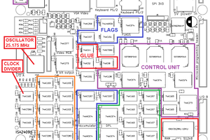
MP-4 is simplest CPU that you can build and run your programs, including conditional branches and a few arithmetic logical operations. As you can see in block diagram, MP-4 is an harvard architecture microcontroller.
In this very first version there is only one register (accumulator). General purpose RAM not implemented yet.
This CPU design is very helpful to understand how CPU's work.
You can easily modify it to add RAM, add more registers or add more instructions.
instruction and operand combined in MP-4 bus. This makes possible less hardware and single instruction in single cycle. Most significant 3 bits are for instruction and lower 5 bits for operand.
total 8 instructions and 32 byte of memory awailable with this configuration.
MP-4 is a MIPS class CPU
74ls181 ALU used for arithmetic and logical operations. 74hc574 used as accumulator.
With this configuration seen in diagram, every results can be stored in accumulator again.
Do not confuse in schematic, it seems there is no direct acces to Acc but its not true
if you arrange 74181's B input to pass data directly out; Data stores in acc directly by passing through 74ls181
74181 may be seen very useful in first look but unfortunately this is not true (its a big mess)
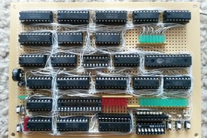
To understand work of this CPU; I recommend setup an 74181 circuit first and play with it a few days. (I did)
74ls181 have two 4 bit inputs, one 4 bit output and 6 control inputs.
this control inputs determines output function.
The main philosophy of MP-4 is simplicity so, I used ne555 as clock generator and its working about 1Hz to understand timing. 555 produces clock signal and 4017 decade clock (I recommend 74hct4017 to compatibility
but I cannot find and used cd4017).
in first cycle CPU fetches instruction to microcode and puts data to bus.
in second phase instruction executing and accumulator refreshing with new value.
MP-4 can run reliably up to 8 Mhz
MP-4 have low encoded horizontal microcode. This mean, we need tons of control pins.
So, I used two 8 bit eeproms microcode sequencer directly reads instruction from ROM data output and produces necessary control signals.
bit 0 and 5-6-7 of microcode1 not used. also LDA and LDM instructions not implemented in this published version.
PcLoad/ signal is producing by zero flag and JP, JPZ signals.
Conditional jump is one of important part of this system.
Acc output goes to 4 input or gates and generates zero flag. zero signal JP signal and JPZ signal
determines conditional or unconditional jumps.
Im putting here pdf version to view and realise your MP-4 also DSN files for Proteus ISIS design suit
in ISIS you can simulate your own CPU design. simply right click on ROM and put your own hex program to run
But please note that Proteus-isis cannot simulate 74181 properly
00 : NOP
20: LDA,n (2 for command, lower nibble is operand: 20,2f, 2a etc all loads acc with low nibble)
40: ADD,n : adds operand to acc
60: DEC : decrements accumulator operand ignored
80 IN A : gets data from input port to acc
A0: OUT A :puts acc content to out port
for in or out commands you may use 4.th bit as adress decoder to add one more port
then BX command puts data to second out port
C0: JP : unconditional jump to adress n (4 bit adress)
Dn: JP unconditional jump to 5 bit adress
En: JPZ : conditional jump to adress n (4 bit adress): jump if zero
Fn: JPZ : conditional jump to 5 bit adress
I used 28c16's for microcodes and 28c64 for main ROM unfortunately proteus design suit cant recognized so that I published circuit with 2764 eproms here is microcodes and test programs
 Anders Dinsen
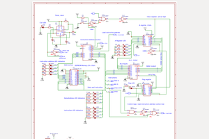
 Szoftveres