Close
0%
0%

CPU4

This is my fourth home brew CPU

Similar projects worth following
My fourth home brew CPU.
Cracked the decoder logic problem.

CPU 4

Background.

Weird CPU

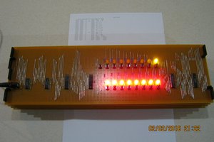
My first CPU (https://hackaday.io/project/12879-weird-cpu) was an 8 bit TTA (Transport Triggered Architecture). It has a front panel and sits happily on my shelf chasing LEDs in circles (such is the life of a simple CPU):

Four bit OpCode CPU

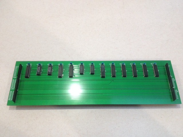
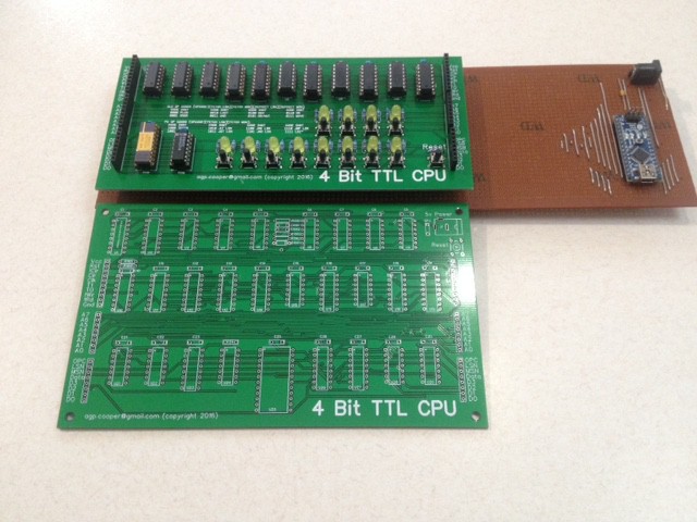
My second CPU (https://hackaday.io/project/13017-4-bit-ttl-cpu) was a 4 bit OpCode CPU. A bit of a disaster, I decided to get PCBs made rather than use strip-board. After 5 revisions (i.e. PCBs) I still do not have it working. I just do not know how many more PCB revisions I will need to get it working.

Subleq CPU

My third CPU design was a Subleq CPU (https://hackaday.io/project/25133-a-subleq-cpu). I quickly realised that it was too inefficient to fit into 8 bits so I moved to 16 bit. This meant I could not use a front panel for programming (i.e. a few hundred bytes is okay but a few thousand words is not!). The decoder started to get complicated as I had to add direct memory access for the programmer (i.e. an Arduino).

Subleq is also very cryptic. So I ported a simple compiler (https://hackaday.io/project/25583-simple-compiler) to export Subleq and wrote a Subleq assembler and interpreter for simulation.

This project too was abandoned as it had migrated so far from an interesting curio to a programming monster. I did learn a lot about compilers and what is expected from the CPU.

CPU 4 Details

CPU 4 is a complete rethink about my home brew CPUs:

  1. I need to use OpCodes for programming efficiency.
  2. I need to radically simplify the OpCode decoding logic.

The usual approach is to use a ROM or a PLA to decode the OpCodes. I have not adopted this approach because I would like to option to convert the design into DTL (i.e. build a transistor CPU).

TTA CPU

I did look at the possibility of using my TTA CPU to interpret OpCodes. It is possible but not well suited for the task. However, if the TTA CPU does not need to access RAM directly then the decoder logic is greatly simplified.

A structure like [DST][SRC] could be used where [DST] is a register and [SRC] is a register.

TD4

TD4 uses this OpCode approach to a degree (https://hackaday.io/project/8442-ttl-based-4-bit-cpu). TD4 also has access to immediate data (which is why it is so interesting) but the approach for immediate data is very primitive. Every OpCode has immediate data attached to it (very inefficient). So adding immediate data on demand would be very useful.
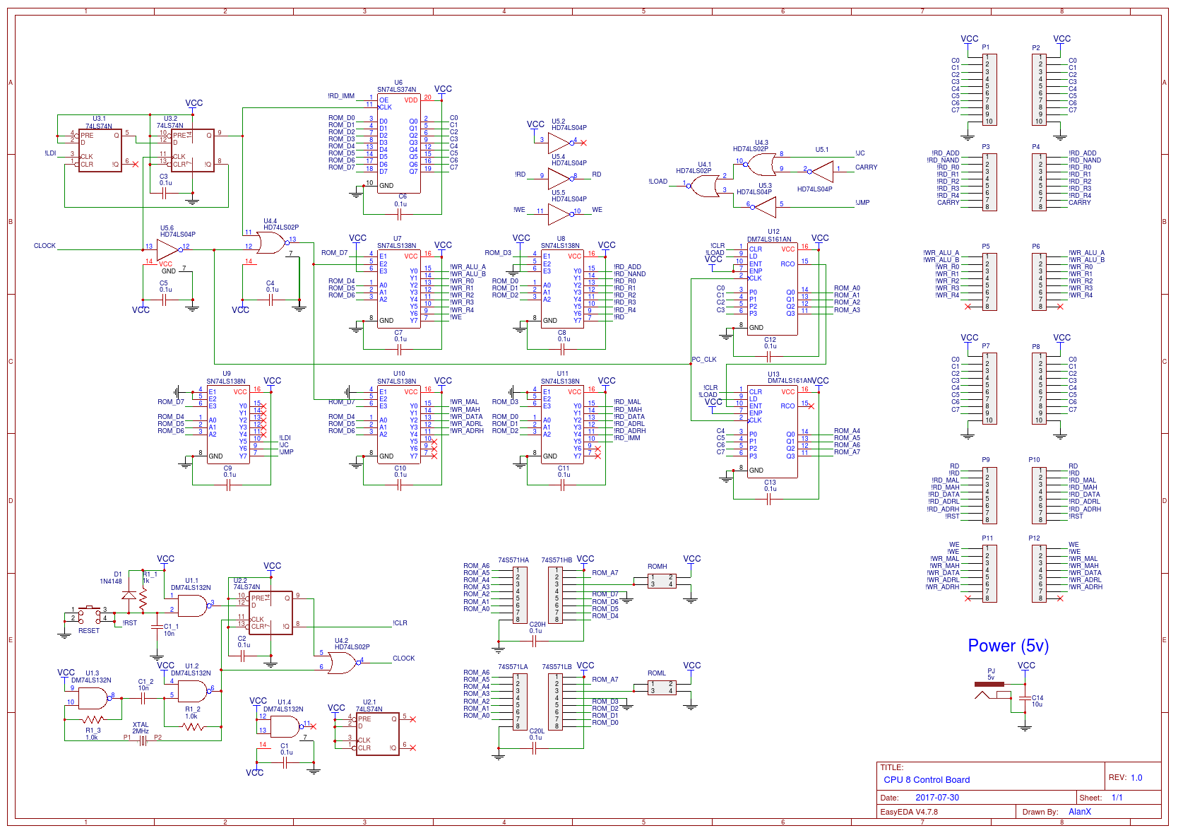
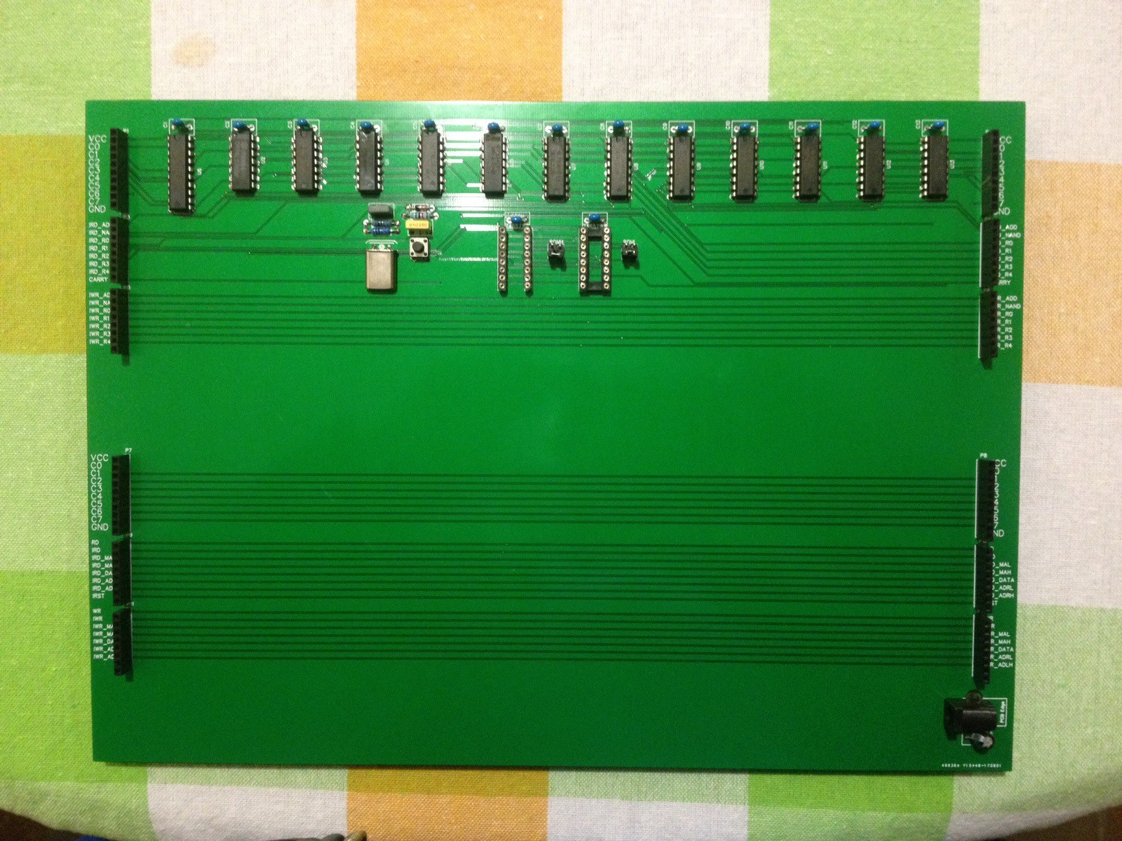
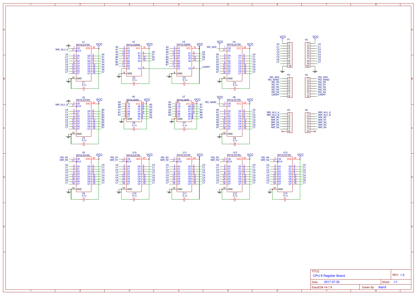
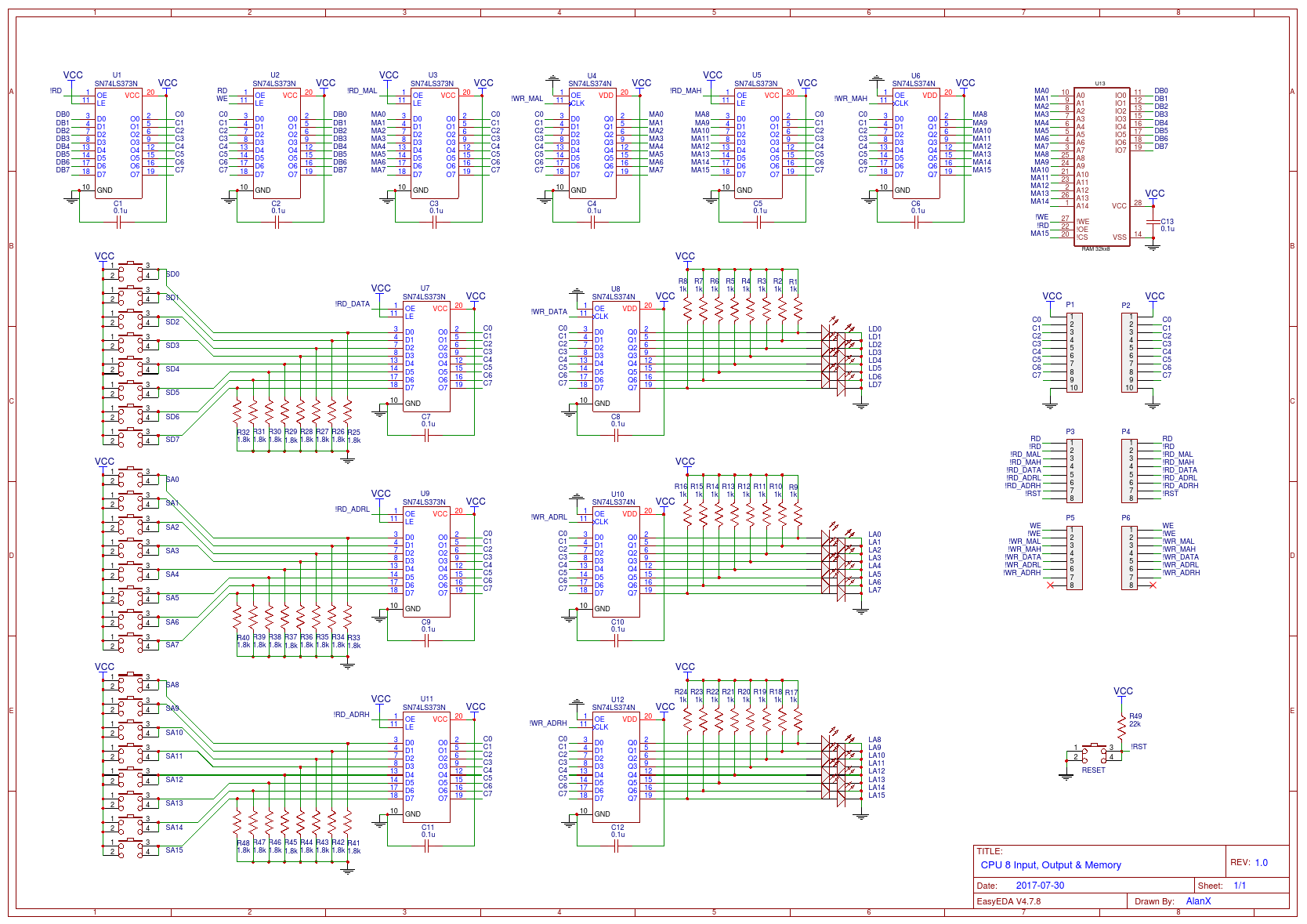
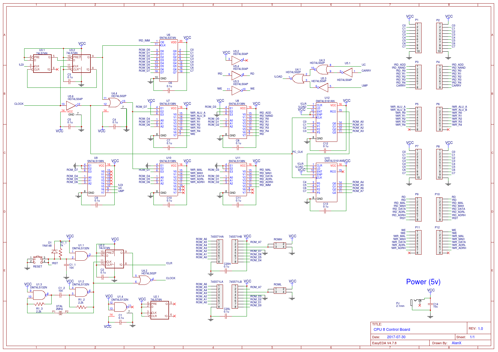
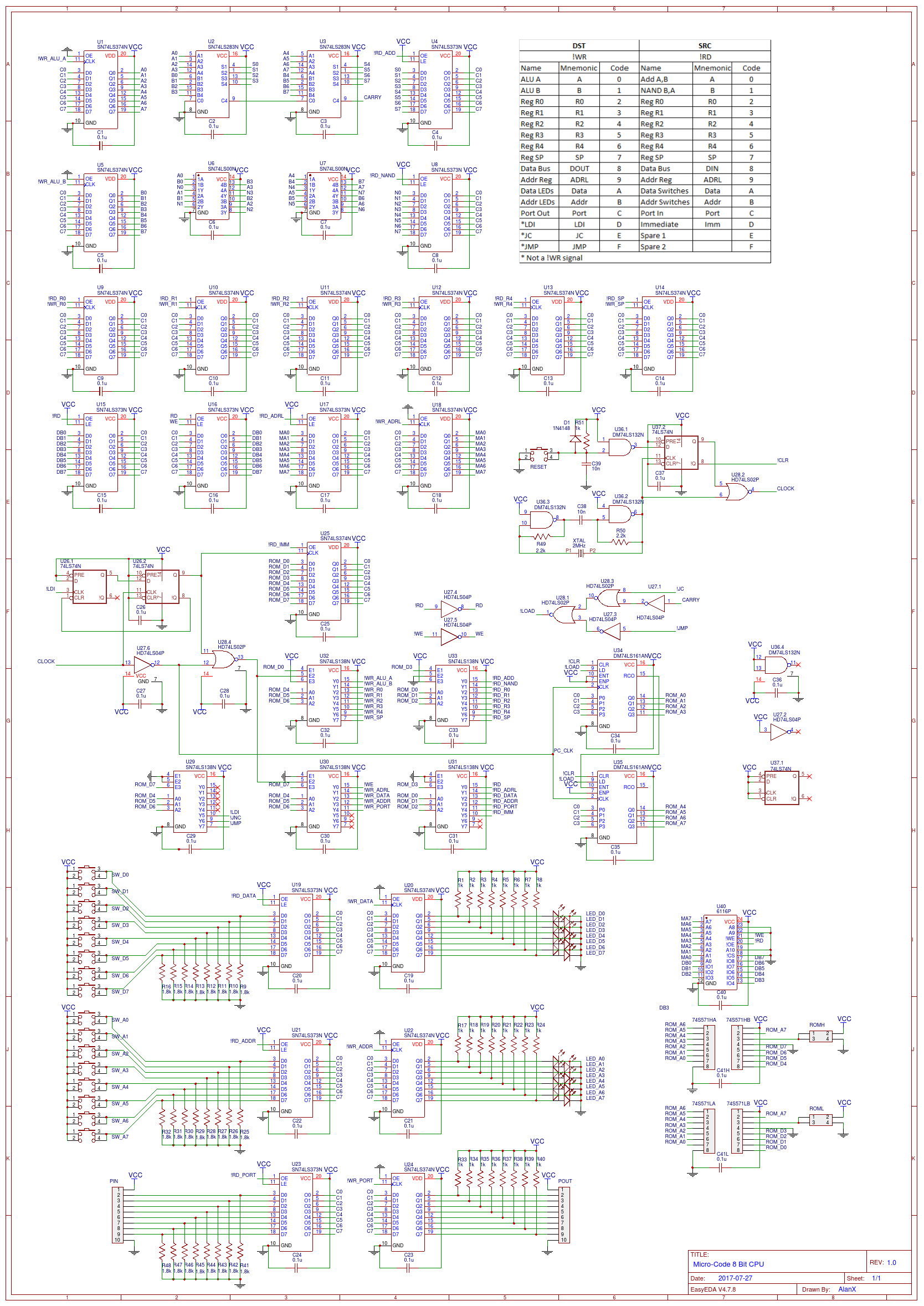
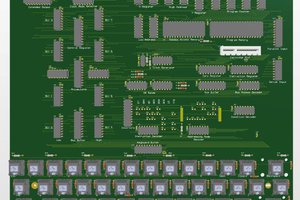
The Decoder

Here is the schematic for the decoder:

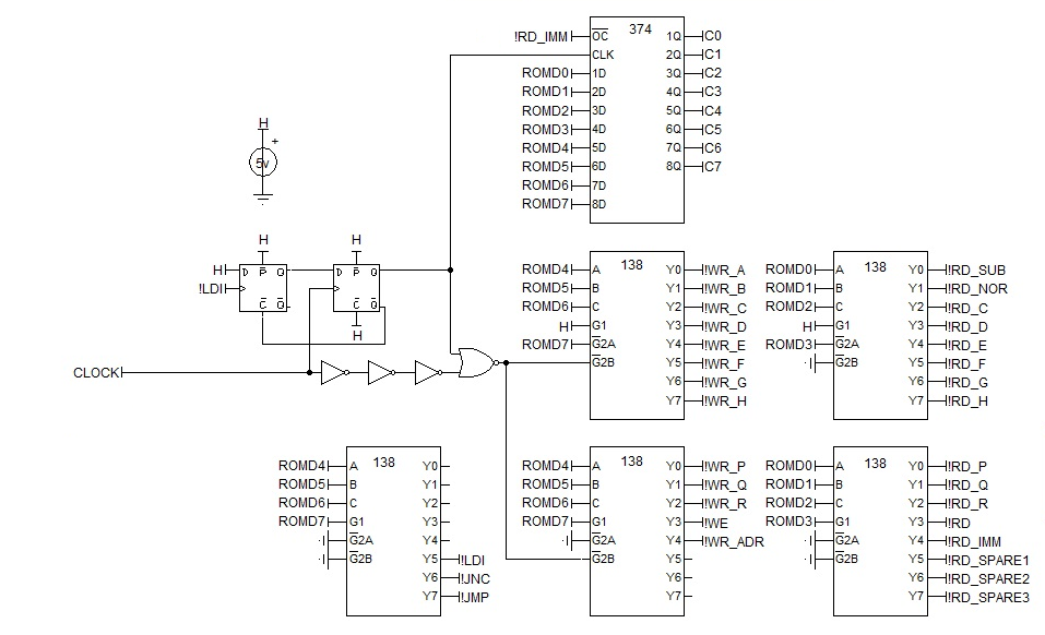
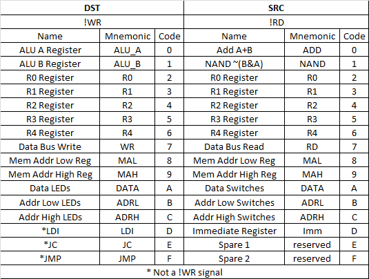
So what you will notice is that I have used 74LS138s to decode the OpCode [DST][SRC].

[DST] is 4 bits (16 options) and [SRC] is 4 bits (16 options). A [DST] is actually a clocked signal while the [SRC] is an out put enable signal. The exception is the three [DST] that are not clocked !LDI (load immediate), JNC (jump on not carry) and JMP (unconditional jump). Very simple is it not!

The !LDI logic blocks the write clock to all the registers (but not the program counter) and instead clocks the 74LS374 latch. This catches the next ROM address as immediate data (if the [DST] decodes to !LDI).

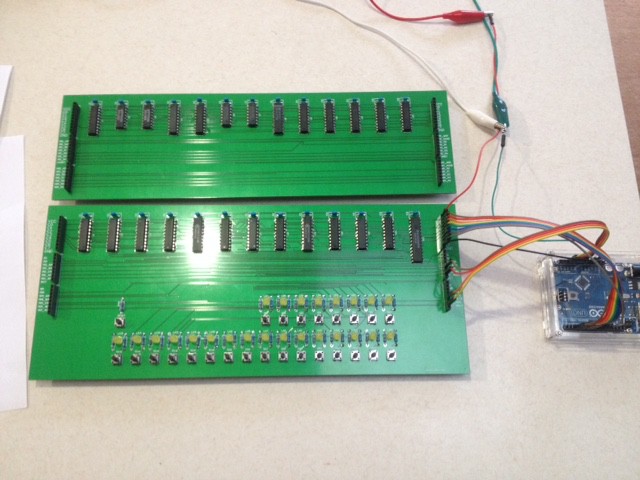
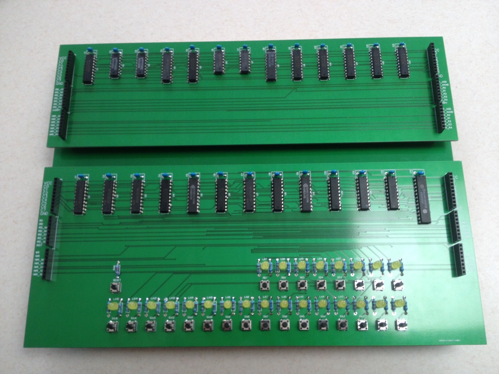
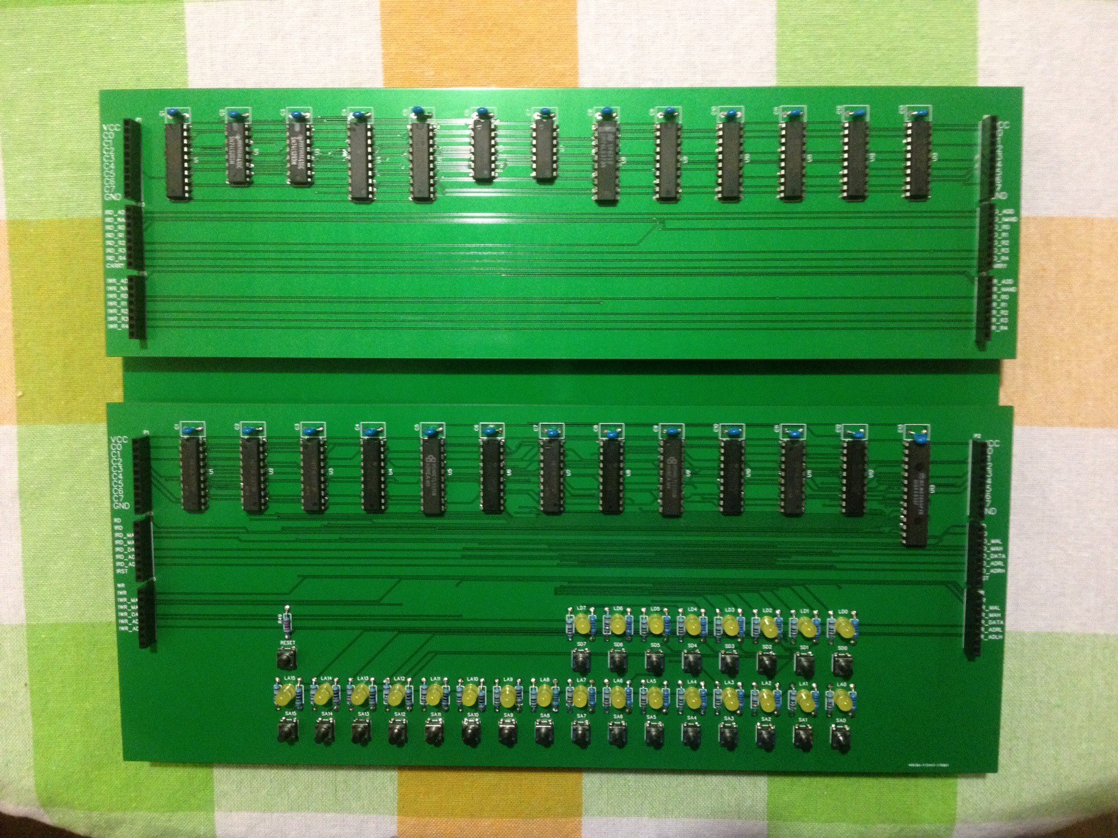
From the schamtic you should be able to see that the CPU can have up to 13 write registers and 16 read registers.
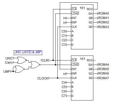
The Program Counter

The program counter is pretty straight forward:


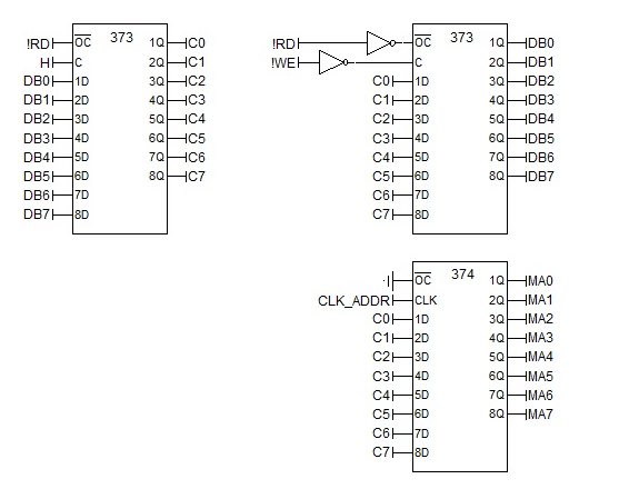
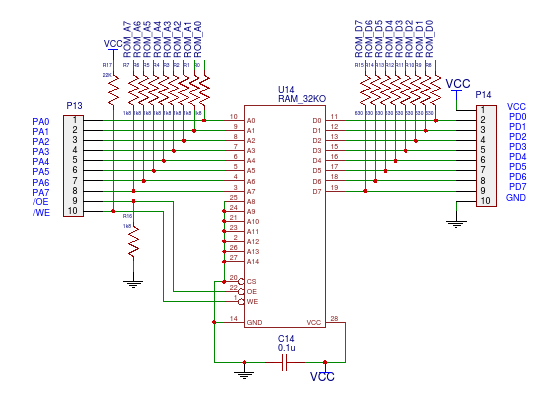
The External Data Bus

For the CPU to access RAM (i.e the user program), the general registers need to configured as read/write:
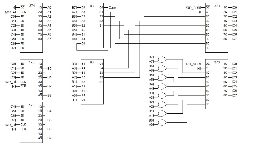

The ALU

The ALU is similar to the Weird CPU but I use integers, subtraction and NOR instead:
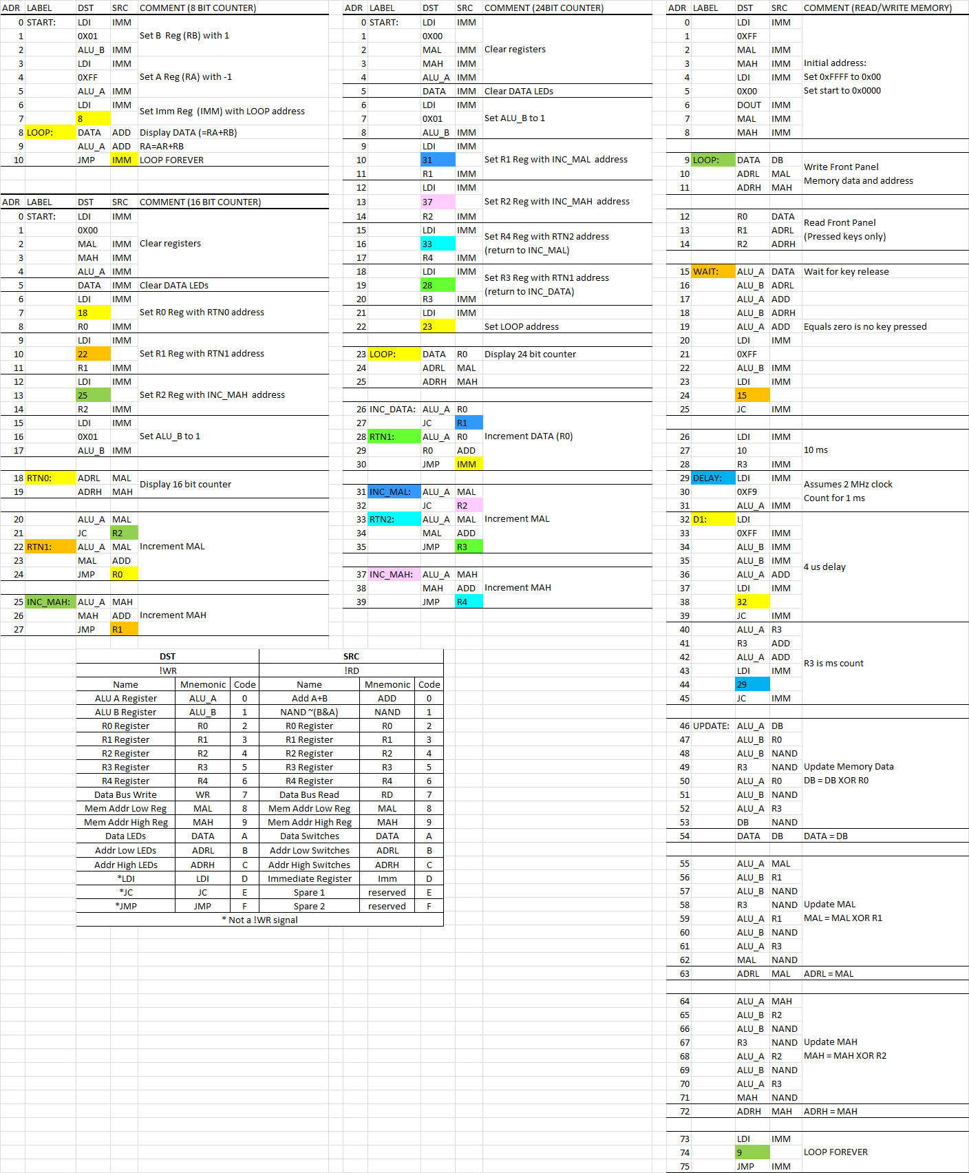
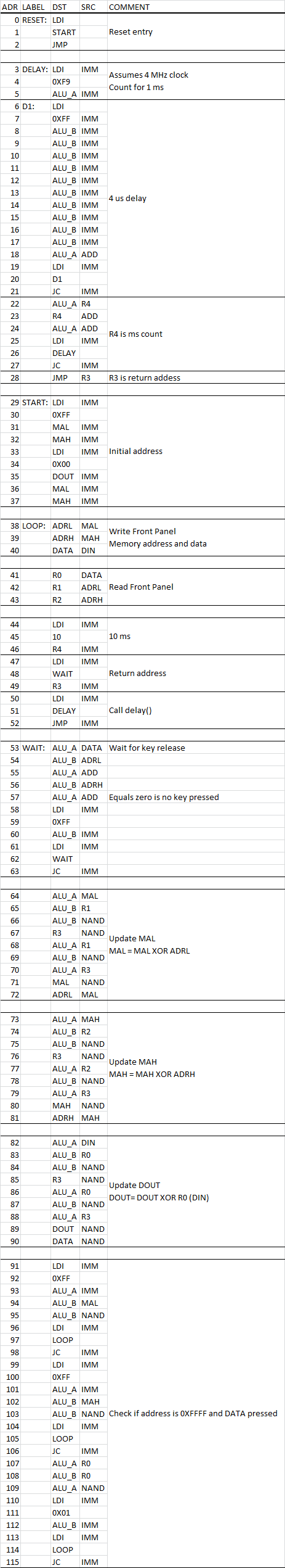
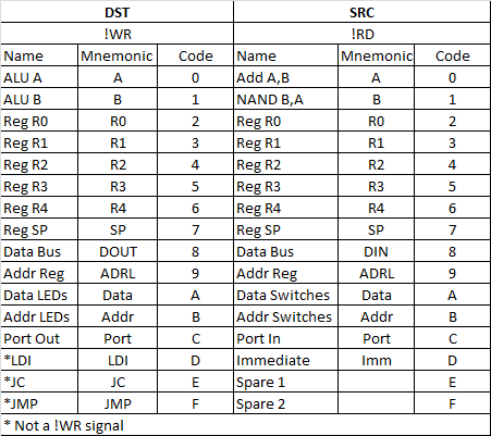
The OpCodes

So here are the OpCodes (these have been updated since my initial post):

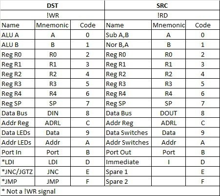
The OpCodes are constructed as [DST][SRC]. So "mov A, B" would be coded as 0x01.

LDI is different as its source is the ROM so the [SRC] and be anything.

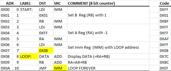
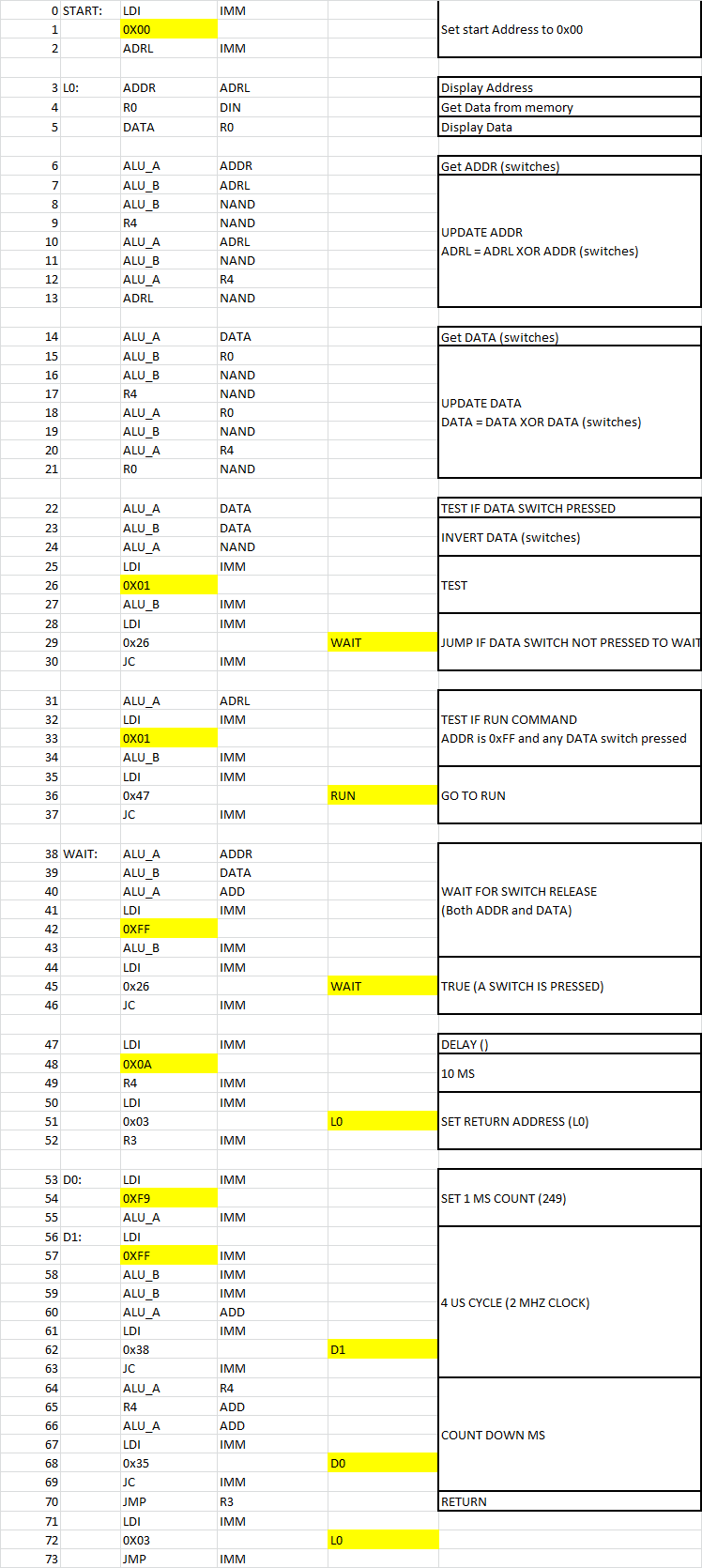
Another example is to increment the C Register:

  • LDI
  • 0xFF ; -1 
  • B, I ; Short for mov B, Imm
  • A, R0 ; Load A with R0
  • R0, A ; Set R0 with A - B which is the same as A + 1 

The above code takes 5 cycle cycles. The Weird CPU (TTA) would take 12 cycles. My Subleq CPU would take 36 cycles.

Reading...

Read more »

tsc - 643.44 kB - 07/30/2017 at 05:50

Download

  • More Debugging

    agp.cooper09/18/2017 at 01:55 0 comments

    More Debugging

    The first issue was that the high PROM has some other data on it. Argh!!

    So a new PROM was burnt.

    The next issue was that the PCB schematic was not identical to the design, so I cut a track and jumped some pins to fix. Later I realised I had made the modification on the fly and had not documented it. I may have to undo the fix (later). Argh!!

    After two days of debugging I realised I had the PROMs swapped! Argh!!

    It now seems to be stuck in the keyboard wait loop (address 0x0F to 0x19).

    Checking the RD/WR sockets I can see signals but they are !WR for !RD, and !RD for !WR.

    Checking the schematic I have miss-labelled sockets. Argh!!

    Another bad board, but at least most of the board is working.

    ---

    New board arrived Tuesday, Assembled it today (I was busy with my Midi project).

    Powered up, partially working. Very erratic. Checked the clock, all over the place.

    Removed the Register Board to get at the Clock chip and everything was good.

    Yes, I know this problem a bad power supply. Swap out the power supply and everything works as it should.

    ---

    Okay, I have a CPU that can display and modify memory. Next is to emulate a CPU such as TTA so it can execute programs. This is purely microcode that has to be written.

    So I have a working CPU (until I find something that does not work!).

    AlanX

  • Revised Control Board

    agp.cooper09/04/2017 at 10:02 0 comments

    Revised Control Board

    I fixed the errors in the old control board but made sure I stayed compatible with the existing daughter boards. I got the PCB back today from the manufacturer.

    Assembled the board and fired it up. Partial success. No smoke, the Data and Address Low switches and LEDs work, Address High not (the illuminated LEDs). This means a lot of the hardware and software is working. This revision has a single step mode so tomorrow I will step through the execution and see if I can workout what is still wrong. With luck it may be a software problem but I am not that confident.

    Read/Write Register A:

    The clock is off, 625kHz rather than 1MHz, but good enough.

    Although I said the Data and Address Low switches and LEDs work, they do but the data is not stored. The correct LED turns on if a switch is pressed.

    AlanX

  • Testing Times

    agp.cooper08/18/2017 at 08:38 0 comments

    Test 1 - No PROM

    Only a problem if the CPU does anything. 

    Nothing happening on the daughter boards but the reset works.

    I took off the Register board to get at the Control board.

    Yes the clock is going but not much else.

    It should be locked into 0xFF or JMP Spare 2.  Spare 2 will read 0xFF.

    So it is locked into an infinite loop at 0xFF.

    All I can confirm is:

    • Clock is present at the PC counter.
    • The PC is Loading (!LOAD is low) 0xFF (actually LS-TTL floating inputs)
    • The decoder is 0xFF.

    So far so good.

    Test 2 - Unprogrammed PROM.

    This should read 0x00 or ALU_A ADD.

    So unless ALU_B is not zero, I should see lots of noise.

    The C Bus counting in unknown steps and the PC counting 0x00 through to 0xFF and rolling over.

    Well the instruction decodes but both the A and B registers always fire up as zero so not much to see. Reset and power up does not randomise. This is a little unusual but not identifiable as a fault at the moment. The pins read as expected (for zero). 

    Took off the daughter boards and the PC is clocking away as it should

    So far all good.

    Test 3 - Burn a Test Code

    Okay I went for broke and uploaded the Demonstration Monitor.

    One last manual check, transferred the hex code the the Arduino and fired up the PROM burner. Error! And again, error.

    What to do? Okay I have a 4 bit Front Panel that I can use to read the PROM.

    Yes it has been programmed.

    Transfer the code back to the spreadsheet I have been using to write the code.

    Check it has written correctly.  All good!

    Okay, I used a old piece of code and I have changed the data sense arrangement on the PROM burner, it probably does not .

    Okay, download the lasted version and no better. But at least both PROMs are coded correctly. I am sure the sense was working the last time I used it!

    I will look at the problem later.

    ---

    Fitted the PROMs and fired up the CPU. Signals but not working. Worse it seems random.

    Bad noise on the !WR_ALU_A signal, traced it back to the clock. The clock is bananas!

    It did settle down but now it is in an infinte loop around 0x00 and 0xFF executing ADD and obviously a JMP. The CARRY signal is active.

    I can pull the crystal and feed in an external clock signal ... tomorrow.

    ---

    The executed code must be:

    ADDR  INST
    0xFF  0X00 (ALU_A,ADD)
    0X00  0XDD (LDI, IMM)
    0X01  0XFF (DATA)

    But the CPI thinks the 0XFF is JMP (JMP 0XFF). The LDI instruction is not working. Well I now know where to look.

    ---

    This is stressful so pack it up and do something else until tomorrow.

    Tomorrow is Today

    Removed the crystal and associated components. Damaged one of the pads (not unexpected with these cheap boards), hooked up a 10kHz schmitt trigger oscillator. 

    Got a pencil, an eraser, some graph paper and my oscilloscope, and start tracing signal through the control board. After three hours I have worked out:

    • The PROM is loaded and reading correctly.
    • The instruction cycle is:
      1. 0xFF 0x00 (ALU_A ADD)
      2. 0x00 0xDD (LDI IMM)
      3. 0x01 0xFF (DATA)
    • The data does appear to be clocked into the IMM register.
    • The DATA (0xFF) is ALSO being interpreted as a JMP 0xFF.
    • There are glitches (they may be absorbed) out of WRITE decoders.
    • I have inverted the PC CLOCK to suit load immediate (LDI) but now the PC LOAD may be too early (i.e. the PC CLOCK too late).

    Redesign Completed

    Too many issues to fix with a jumper or two. Redesigned the CPU control board, addressing all the issues identified. Some additional enhancements as well. The OpCodes have changed so the old PROM is now useless.

    Fixed:

    • the jump problem
    • the write glitch
    • the PC load issue
    • the clock (it is now a schmitt trigger)
    • added JNC and RD_PORT to the OpCodes
    • made register A read/write
    • made register B read/write

    Cost was one additional chip (a 3x 3 input NOR gate). 

    The OpCodes (Version B) are now:

    So I can now store data temporarily in the ALU without penalty.

    The other reason for the rearrangement is so that it is more PROM reuse friendly.

    Here is some code for an 8 bit counter:

    Back to CPU4A

    I finished...

    Read more »

  • Monitor Time

    agp.cooper08/13/2017 at 09:00 0 comments

    Monitor Time

    Time to code the monitor program. Too late to use simulate RAM (unless I have no choice and even then a Nano does not have enough output pins), it is about getting the code to work first time. Yes, well if I am lucky! To help I will write the same monitor code is Pseudo C Code and as commented machine code.  

    OpCodes

    Here are the updated OpCodes:

    The main risk is that JC is JNC so I will double check:

    It looks okay, a !JC (low) and a CARRY (high) forces !LOAD low.

    Subleq Emulator

    Started writing the emulator, its starting to get complicated with an 8 bit data bus and a 16 bit address space.

    The programming of the PROM needs a rethink! The Nano does not have enough output pins to emulate/control the CPU and the micro-code is too big to get right the first time.

    I think the immediate objective is to prove the CPU works rather than get the CPU working to final specifications. In order of complexity:

    • An 8 bit counter.
    • A 16 bit counter.
    • A 24 bit counter
    • A front panel but no emulator.

    Here are the codes for the options:


    The cut down monitor code looks good to me. It is code I have spend some time working with. A successful run is all I want as the Control board needs to be rebuilt.

    The next version of the control board will support a Flash PROM and a way of programming in-circuit. I will replace the Flash ROM with the TTL PROMs when all debugged (want to stay with the TTL style).

    Micro Code

    Now that I have worked out how to construct simple call/return (see the 16 and 24 bit counters), coding the CPU is more pleasant. I hate using JC when I need JNC (using JC and JMP) as it takes six instructions instead of three if using immediates).  It can be done but I will lose a register. Pleasant coding is winning at the moment.

    In Circuit Programming of the Flash Memory

    Rather than use two PROM which have to be programmed in a specially designed programmer, I want to in-circuit program a flash memory chip.

    I can do this by isolating the flash chip with series resistors. Currently the PROMs have:

    1. one LS-TTL output to the PROM address bus (i.e. 74LS161s)
    2. 2-3 inputs reading the PROM data bus (i.e. 74LS138s).

    Standard LS-TTL Specifications:

    • VIL 0.8v max
    • VIH 2.0v min
    • VOH 2.7 min (3.4 typ)
    • VOL 0.5v (max) (0.35 typ)
    • IIL 0.36mA
    • IIH 20uA
    • IOL 8mA
    • IOH 400uA

    Case 1 Resistors

    The value resistor is 1.2k:

    • 6.5k = (3.4 - 0.8) / 400u (output high)
    • 1.2k = (0.8 - 0.35) / 0.36m (output low)

    The datasheet is rather conservative. Measurements suggest 0.20mA rather than 0.36mA (consistent with the LS-TTL schematic showing an 18k to 20k internal pull-up resistor). The maximum resistor in this case is 2.2k. To be safe I will use a 1.8k resistor.

    The programming current (I1) from the Adruino would be 2.6mA (=(0.8v - 0.3v) / 1.8k).

    Case 2 Resistors

    Same as above but 1/3 of 1.8k (or 630R) .

    The programming current (I2) from the Arduino would be (when the output is an input) -800uA (to the Arduino). Enough to pull down 4 gate inputs (at 200uA per gate) (=(0.3v - 0.8v) / 630).

    Here is the schematic of the in-circuit flash RAM:

    No it will not work! Here is another version:

    JA is the Arduino Address and JD is the Arduino Data. The first 74LS04 will have to source up to 4.8 mA. As the input low current is only 10uA for the Flash RAM I can increase the input resistor values network up to 20 times. This circuit pull 640uA from the output:

    All good now! 

    The Plan

    The plan now is to:

    • Code the 16 bit counter in one page of the PROM
    • Then the demonstration monitor in the other page of the PROM.
    • If all good then a new set of boards using a smaller footprint and the Flash RAM.

    I have already redesigned for JNC and JC conditional jumps.

    A Stack

    What this CPU needs is a stack. The first version is a short (8 bit) stack:

    /*
     * PUSH R0
     *    CALL WITH "JMP IMM" AND RETURN WITH "JMP RTN"
     *    SP = R3
     *    RTN = R2
     *    SP = SP - 1
     *    MEM[SP] = R0
     *    RA AND RB DESTROYED
     *    17 INSTRUCTIONS
    */  
    DST   SRC
    ===   ===
    //    DECREMENT SP
    LDI   IMM
    0XFF
    RB    IMM
    RA    SP
    //    SWAP MAL AND SP
    SP    MAL
    MAL   ADD
    //...
    Read more »

  • Construction

    agp.cooper08/06/2017 at 09:20 0 comments

    Construction

    My boards are back. I erred on the side of big for these boards. The Control Board has two piggy back daughter boards. I when big so that the auto router would work. But it was costly (almost double what I paid for my 4 bit CPU on a same same basis:


    Okay, the view distorts the relative sizes but you get the idea.

    I think I am on the right path but instead on the headers being vertically aligned (as show below) they should be in horizontal rows. Then each daughter board would be long and narrow:


    This is the register board, you can see how confident I am, no IC sockets!

    Here is a close up of the 4 bit CPU Front Panel (in the Arduino test-bed) above the main CPU board:


    The Front Panel is working but I have yet to write a simulator to test the monitor program (or assemble and test the CPU board).

    So other than buying some more component to finish off the other two boards I need to test each board to make sure they are working as expected.

    The Wind Is In My Sails

    Not often I have this much go right. Both daughter boards work fully. The only error on the boards a label I wrote "!WR_ADD" and "!WR_NAND" instead of "!WR_ALU_A" and !WR_ALU_B".

    Magic!

    The Control Board has one fault (so far). I have offset the Front Panel Board (i.e. I/O/Memory board) header pins about 1/2" too far down. It is cosmetic.

    Here are the two completed boards (and the Arduino I used to test the boards):


    Stop

    I assembled the clock this morning on the Control board. Power up but no signal. Actually the scope said negative. Powered down and checked the ICs to see if they were hot. On was warm. Now I have done this before - hooked up the power jack the wrong way in EasyEDA. It happens when EasyEDA change their component library and I have to fine new components, it causes all sorts of problems. But this is partially my fault as I hooked it up wrong.

    Pulled the power jack, cut off the middle tab and refitted it in reverse. Powered up, now I have a clock signal but it has sub-harmonic digital noise. I am using an unusual clock circuit in that I use schmitt triggers instead of simple gates. The bread-boarded version of this circuit works fine so I assume the 74LS132 is damaged (pretty likely).

    Here are the boards after I stopped working on i:


    And a trial fit:


    Note the gap between the daughter boards.

    There are enough errors in the Control board that I will update the PCB and get it remade.

    Review

    I was not that happy with the diagnosis for the clock so I had another look.

    First I did not have any 2.2k resistors so I used 2.7k resistors. An easy check would to replace them with 1.8k resistors. The 2.2k resistors were on the high end for LS-TTL based on my research. I got a big improvement but still some weird clocking with extra cycles (sub-harmonics). So I dropped the resistors to 1k by paralleling the 1.8k resistors with the old 2.7k resistors. All good!

    Pulled to resistors and replaced them with 1k resistors, but no:


    I cleaned up the PCB and checked for shorts. The resistor pad was damaged and shorting to ground. Unsoldering plate through holes is a real problem with low cost PCBs. Bridged the damage, but the output was bad:


    Also note that the waveform floor is about 0.5 volt (too high). In the beginning the floor was lower and the mini-hill higher, after a while the waveform settle to this:


    Note how high the floor is (nearly 1v), clearly the short damaged the output drive and I was watching output drive fail. 

    The Control Board

    Other than some ringing on the clock signal (which does not seem to upset things), the PC is happily counting away and the reset works. Although the rest of the circuit in not complicated I cannot test it. The clock is too fast for the Arduino. Originally I was going to have a jumper on the crystal so I could inject a low frequency for test purposes. It never happened. Now I have to test it via the ROM!

    The controller board:


    The assembled CPU less PROM:

    AlanX

  • Monitor Program Update

    agp.cooper08/02/2017 at 05:37 7 comments

    Monitor Program

    I have rewritten the monitor program for a 16 bit address and a 4 MHz clock.

    Still needs to be simulated before burning to PROM:

    You get a feel for just how primitive these simple CPUs are from the code above.

    The CPU OpCode interpreter would commence on line 116.

    AlanX

  • PCBs

    agp.cooper07/30/2017 at 07:33 0 comments

    PCBs

    The problem with PCBs is that one mistake and the board is useless.

    So divide and conquer, I have divide the CPU into three boards:

    • Registers
    • Input, Output and memory
    • Control and ROM

    I need the Input and Output board in order to debug the monitor program.

    Here is the Register Schematic:

    The Input, Output and Memory schematic:

    The Control and ROM board:

    Note that the first two schematics (boards) will piggy-back off the control board.

    Support for 16 bit address space

    I gave in to temptation and made support for 16 bit address space.

    PCBs Designed

    Completed the three PCBs:

    • Control and ROM
    • Register
    • Front Panel (input/Output) and RAM

    One last check of the schematics and then send them off for manufacture.

    Checked the schematics this morning and found some more errors. Fixed.

    Now this is the problem with PCB design, the errors. Five years ago my "bug detect" eyesight was better but today I could trip over a bug! Anyway, the only way to find out now is to get them made.

    Next Generation CPU

    If there is a next generation, then I would push the I/O into memory address space as it would free up three CPU registers. One of those registers I would use as a page register so that the micro-code ROM could be expanded to 64k.

    AlanX

  • Schematic Debug

    agp.cooper07/26/2017 at 14:40 0 comments

    Schematic Debug

    I don't have very good tools to test my schematics but Tina can be coerced into something and something is better than nothing. Most the errors I find error are label errors but some of the Tina models are also wrong.

    Spend the day testing the CPU. Found lots of schematic error (mostly labels but also swapped internal bus lines). Not surprisingly you cannot read and write at the same time to the same register unless it has been designed for it (i.e. the Data Bus and the ALU). But the ALU only works because the gates between the input and output buffers delay the propagation just enough. But still the 74LS374 are edge triggered so it may be a Tina model problem.
    I have changed the ALU to ADD and NAND as CPU internals are not seen on the external bus (i.e. no advantage to working with signed integers inside the CPU). 

    Adding More Register

    Does not seem to be any point not fully populating the registers. No real saving leaving them out. This CPU does not have enough registers (or ROM) to model an Intel 8080 nor enough ROM to decode all the instructions (a 12 bit version might but a 16 bit version certainly could).

    Updated OpCodes

    From the opcode table you can see I have packed a lot in, but I have resisted the temptation to add 16 bit support (next time):

    The Plan

    The plan at the moment is to code the front panel interface directly in the CPU micro-code and to model Subleq as the first CPU model. This allows me to stay with 8 bit with Subleq. Something that I could not do with a straight Subleq CPU.

    Vero Board

    I have knocked up the ALU on a Vero Board. But this is expensive and I will need at least two more boards. The big advantages with Vero Board is that mistakes can be fixed. The down side is a board this size would take a full day to make and it is very tedious:

    EasyEDA PCB

    EasyEDA is not too hard but one error and the board is useless. That was the problem with the 4BitCPU. But in this case the decoder is much simpler and you do get better at designing PCBs each time you try. I seem to have talked myself into a PCB again!

    More Schematic Errors

    Spent the day entering the schematic into EasyEDA. Saw that the PC clock was the wrong phase I had inverted the signal. Here is the fixed clock simulation:

    It looks right to me.

    Micro-Code ROM

    I am using a two 74S571 PROM which are 4 bit and 512 words each but only 256 words are accessible with an 8 bit bus, unless I use a page register (perhaps later). I will use a 6116 SRAM for memory but I am resisting the temptation to add a high address for the time being. So only 256 words are accessible. Here is the current EasyEDA schematic:

    Its is pretty big so I want to spend a day or two checking it.

    It is pretty clear I will have to split this schematic into three boards:

    • Registers
    • PC and control
    • IO and memory

    Monitor Code

    Spent some time coding a monitor program. The code is very similar to the Weird CPU.

    I also wrote an interpreter for the code but it is a bit tricky. If I print the registers for each step, the delay routine spits out ~25,000 lines alone. Really I need to use an Arduino and a front panel but I don't have a front panel.

    Anyway here is the monitor code:

    Looking at the code after I have loaded it I seem to have forgotten to save the updated data back to memory!

    AlanX

View all 8 project logs

Enjoy this project?

Share

Discussions

agp.cooper wrote 07/29/2017 at 09:44 point

Hi BigEd,
Yes and no. I reverted back to ADD and NAND, and to JC (rather than JNC).
It was slightly more efficient and I don't need integers inside a CPU.
I spent the day coding different versions of the monitor program and selected the option with the least number of code lines. I also un-inverted the input switch logic as well. Currently the monitor is about 57% of the Weird CPU (TTA) code and eight times faster, but that is inside the CPU.
Subtraction is Turing complete and well suited to next step up (compare etc.) but at the CPU level it does not really matter as I just use the NOT of the constant etc. in a test.
I was considering subtraction because I have written over a thousand lines of Subleq code that I could use for the OpCodes. But I need more ROM capacity for this. So rather than get too ahead of myself I have limited the scope of the project.
Regards AlanX

  Are you sure? yes | no

Ed S wrote 07/29/2017 at 12:47 point

Fair enough - good idea to keep calibrating the machine against real code. I have a soft spot for Reverse Subtract as a primitive, but it hasn't yet made it into our CPUs...

  Are you sure? yes | no

Ed S wrote 07/29/2017 at 08:22 point

Subtraction and Nor? Good choices! I like it already.

  Are you sure? yes | no

Yann Guidon / YGDES wrote 07/29/2017 at 07:31 point

I'm very, very, very curious about this one :-)

  Are you sure? yes | no

Similar Projects

Does this project spark your interest?

Become a member to follow this project and never miss any updates