0%
0%
Vector Network Analyzer
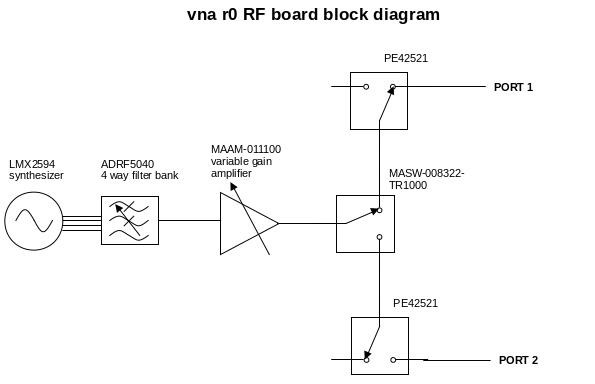
open hardware 2 GHz to 13 GHz two-port vector network analyzer
 Jon Klein
Become a Hackaday.io member
Already have an account? Log in.
Just one more thing
To make the experience fit your profile, pick a username and tell us what interests you.
Pick an awesome username
hackaday.io/
Your profile's URL: hackaday.io/username. Max 25 alphanumeric characters.
Pick a few interests
Projects that share your interests
People that share your interests
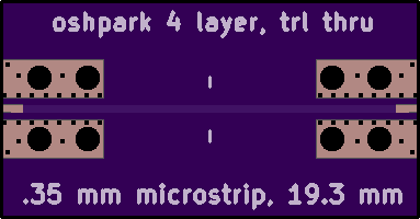
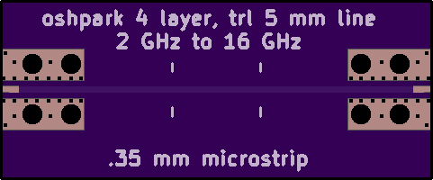
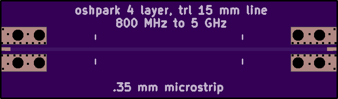
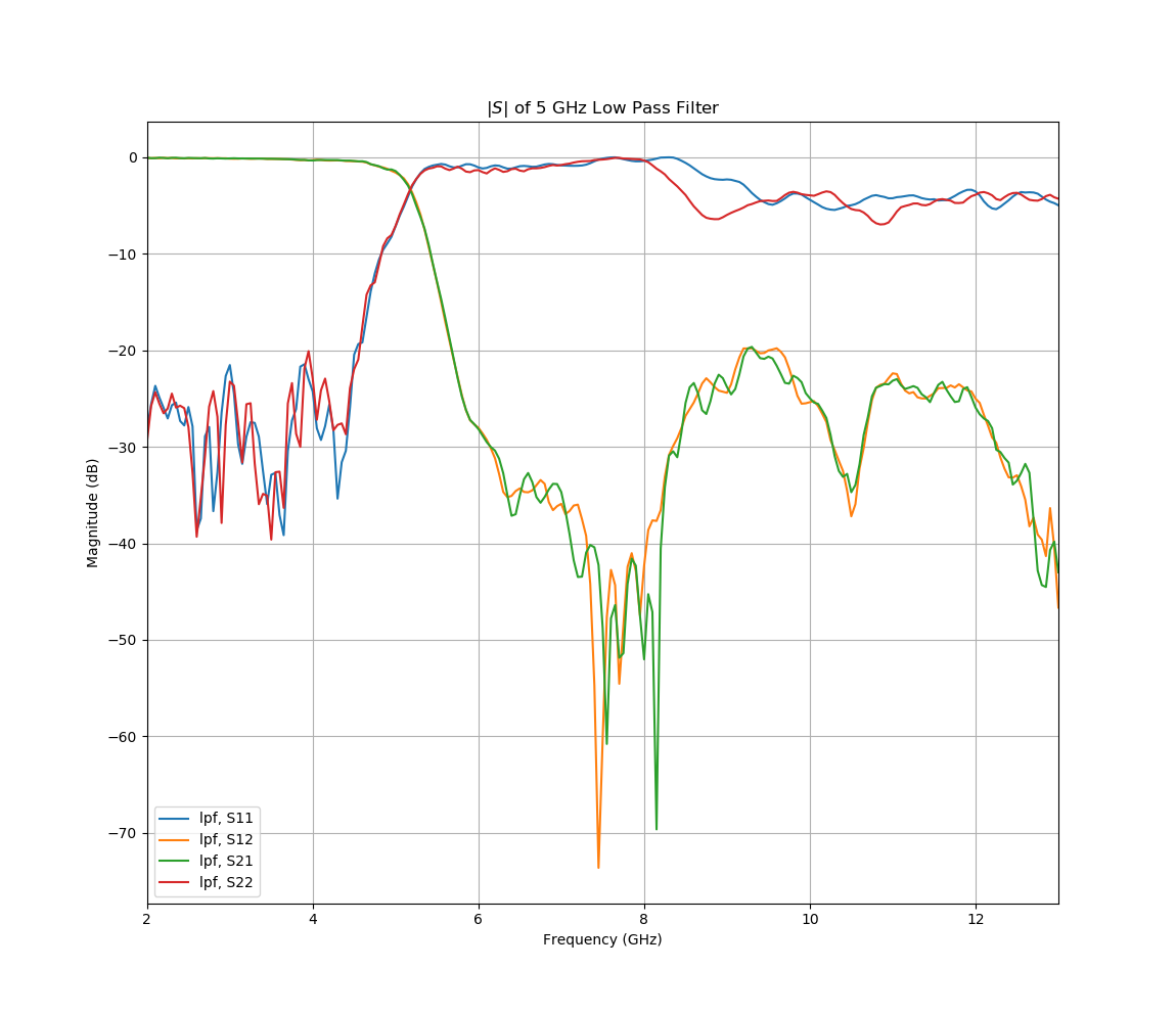
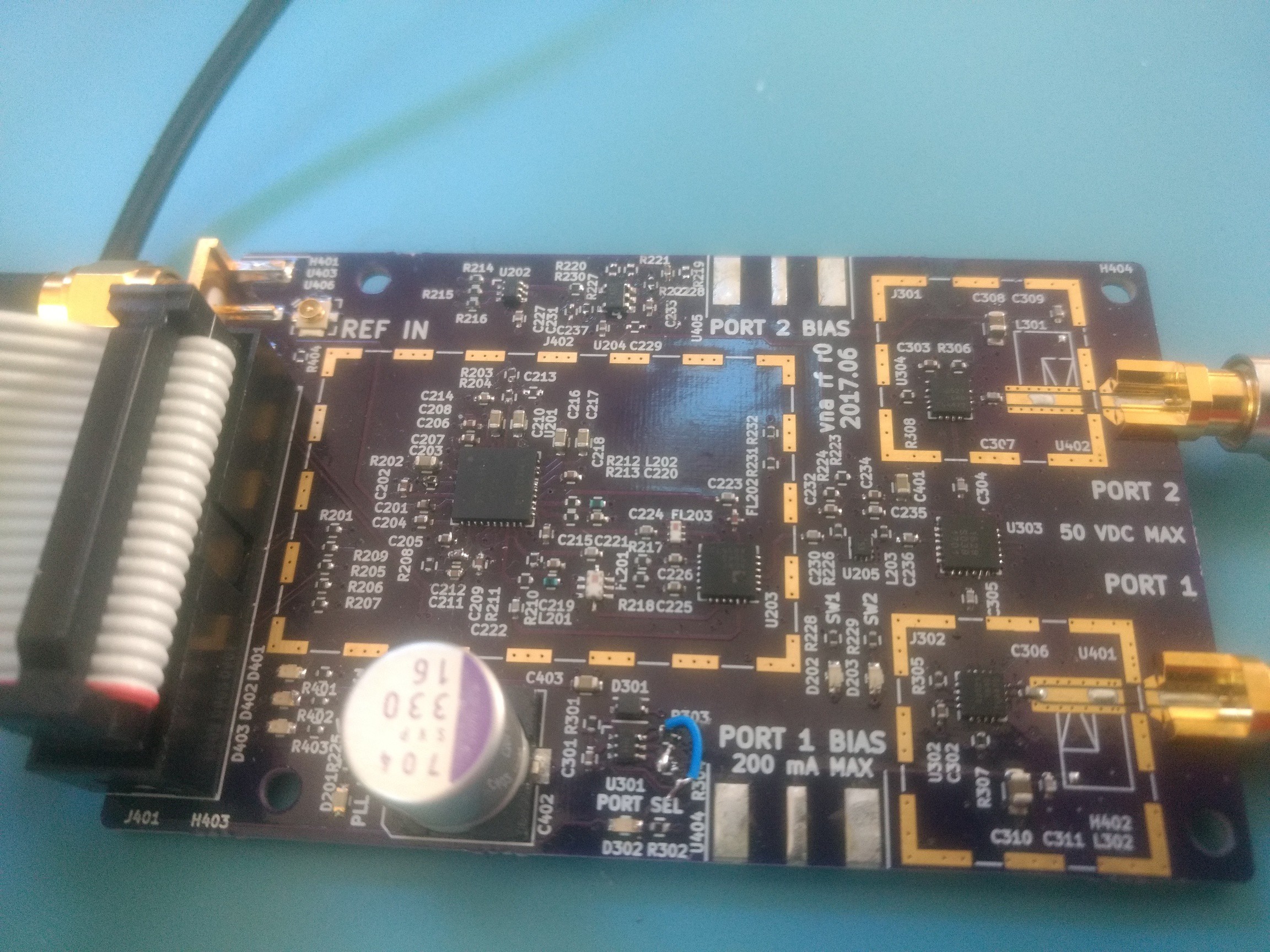
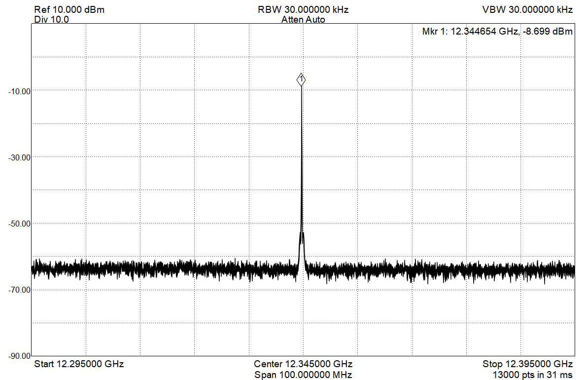
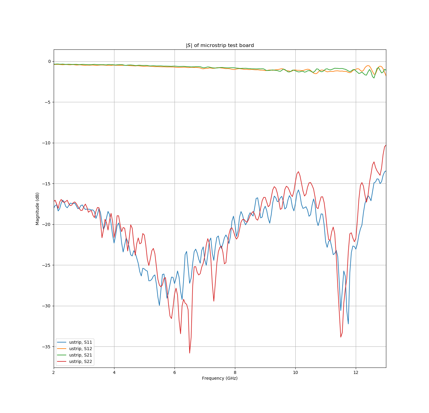 It looks.. okay. S21 at 10 GHz is about -1.2 dB, and S11/S22 are generally below -15 dB out to about 12 GHz. Running the OSH Park 4 layer stackup through the qucs line calculation tool, I would expect about .65 dB of attenuation through the microstrip. If that is correct, it leaves about .3 dB through each of the
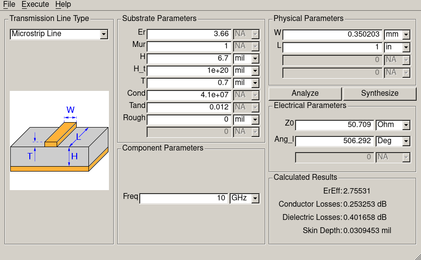
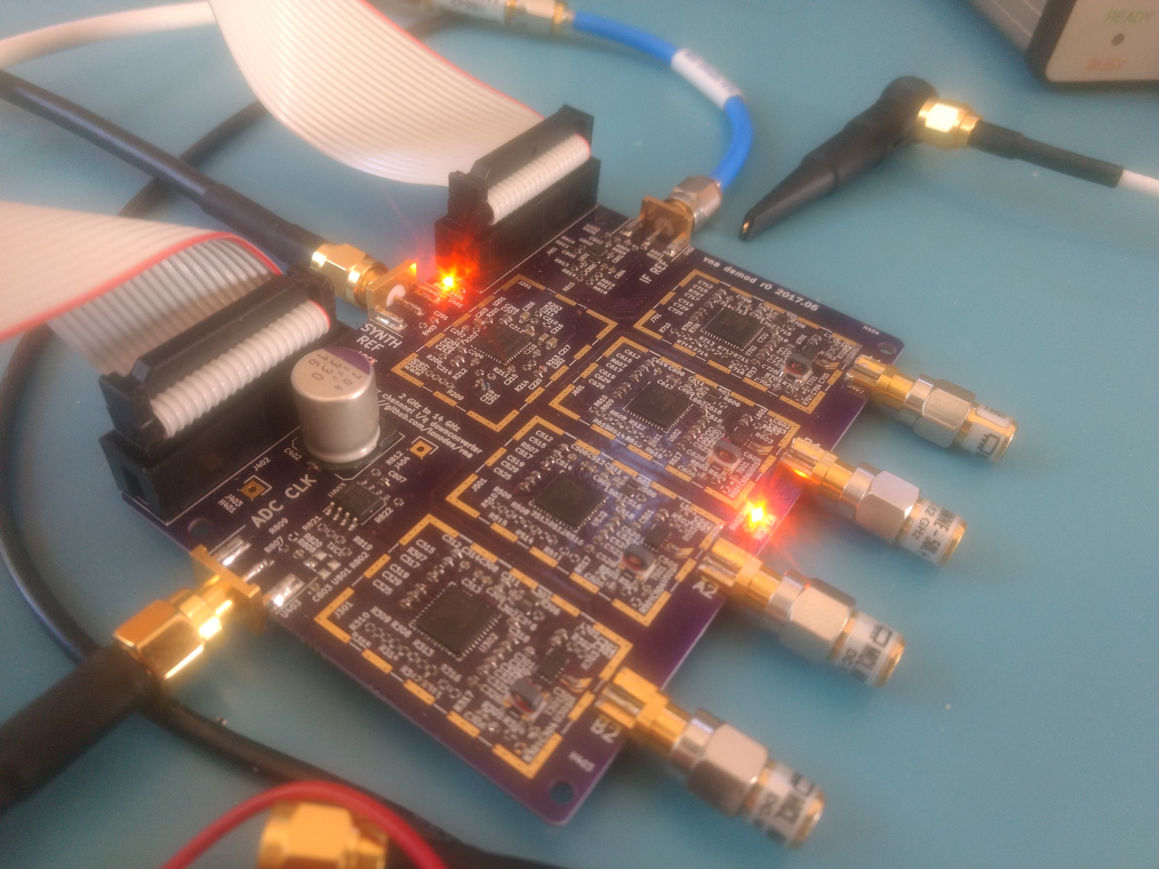
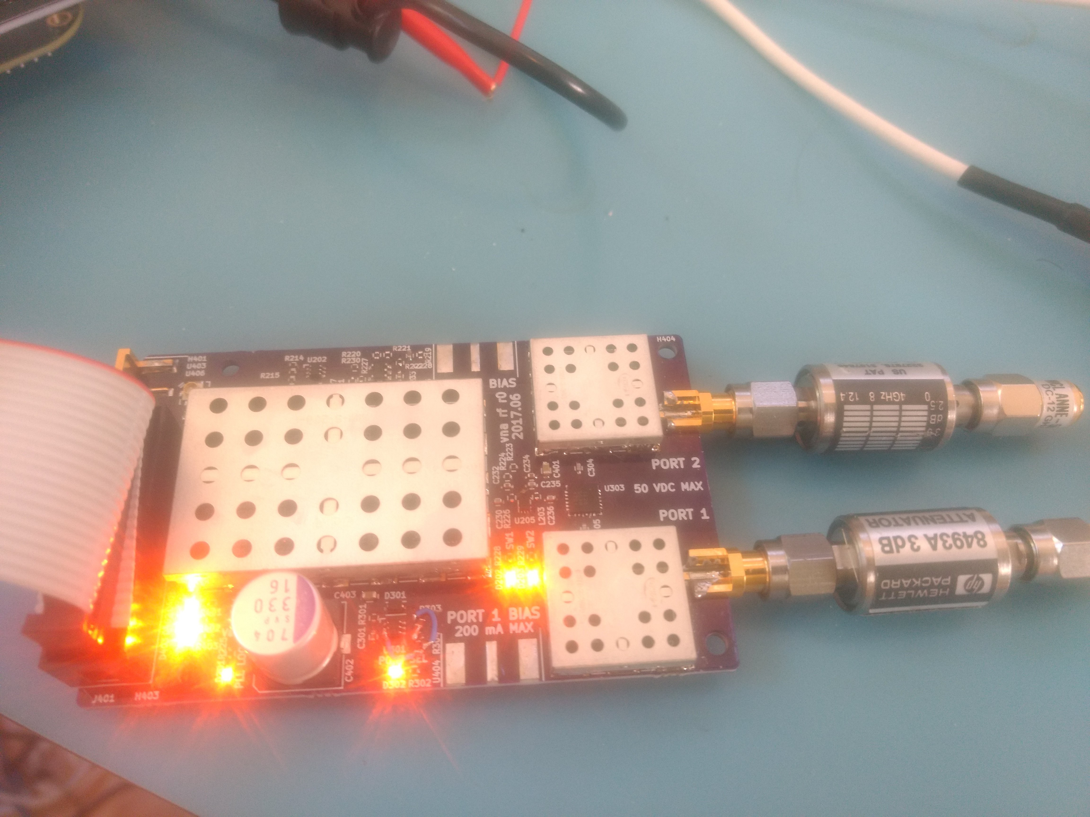
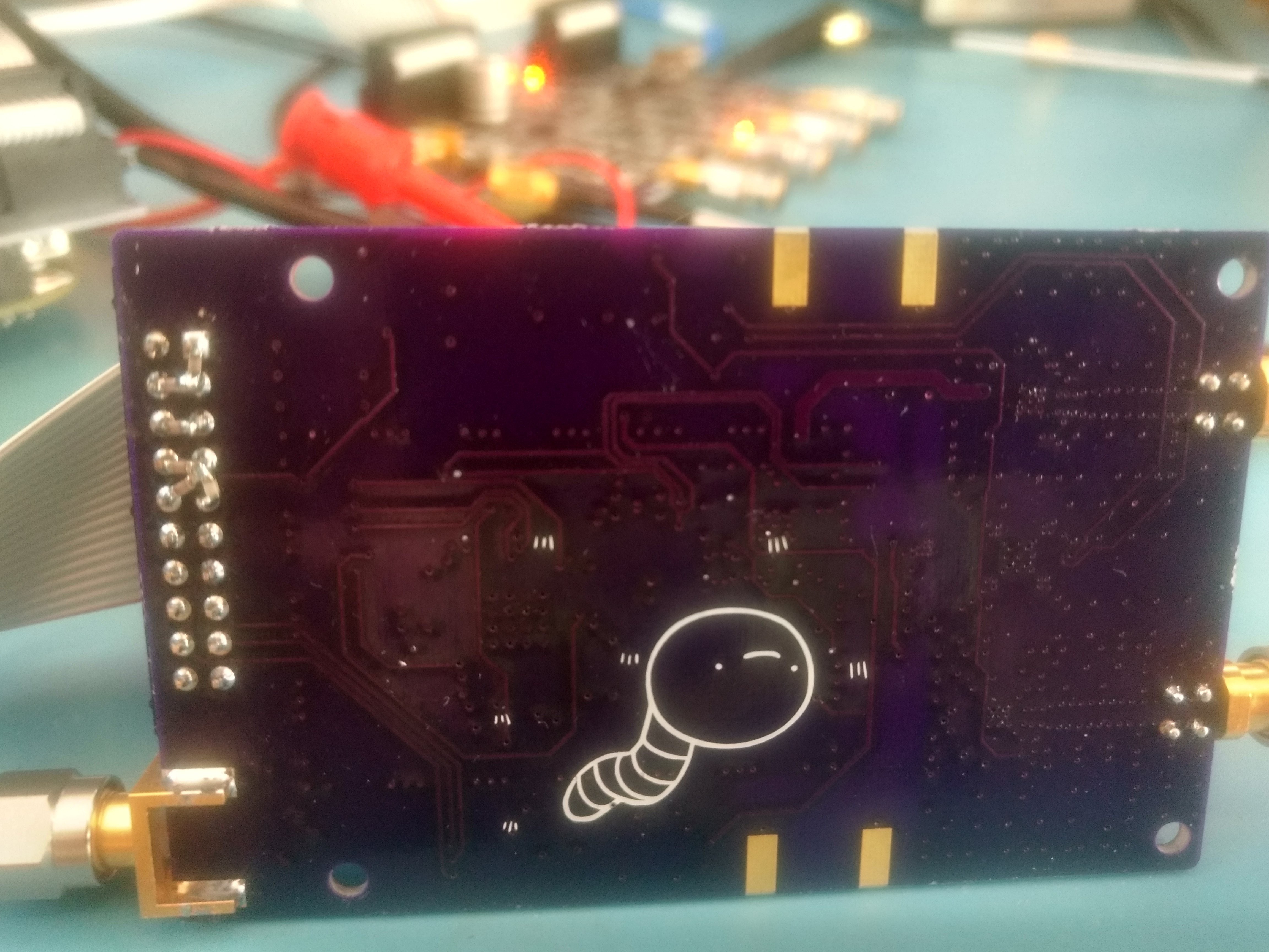

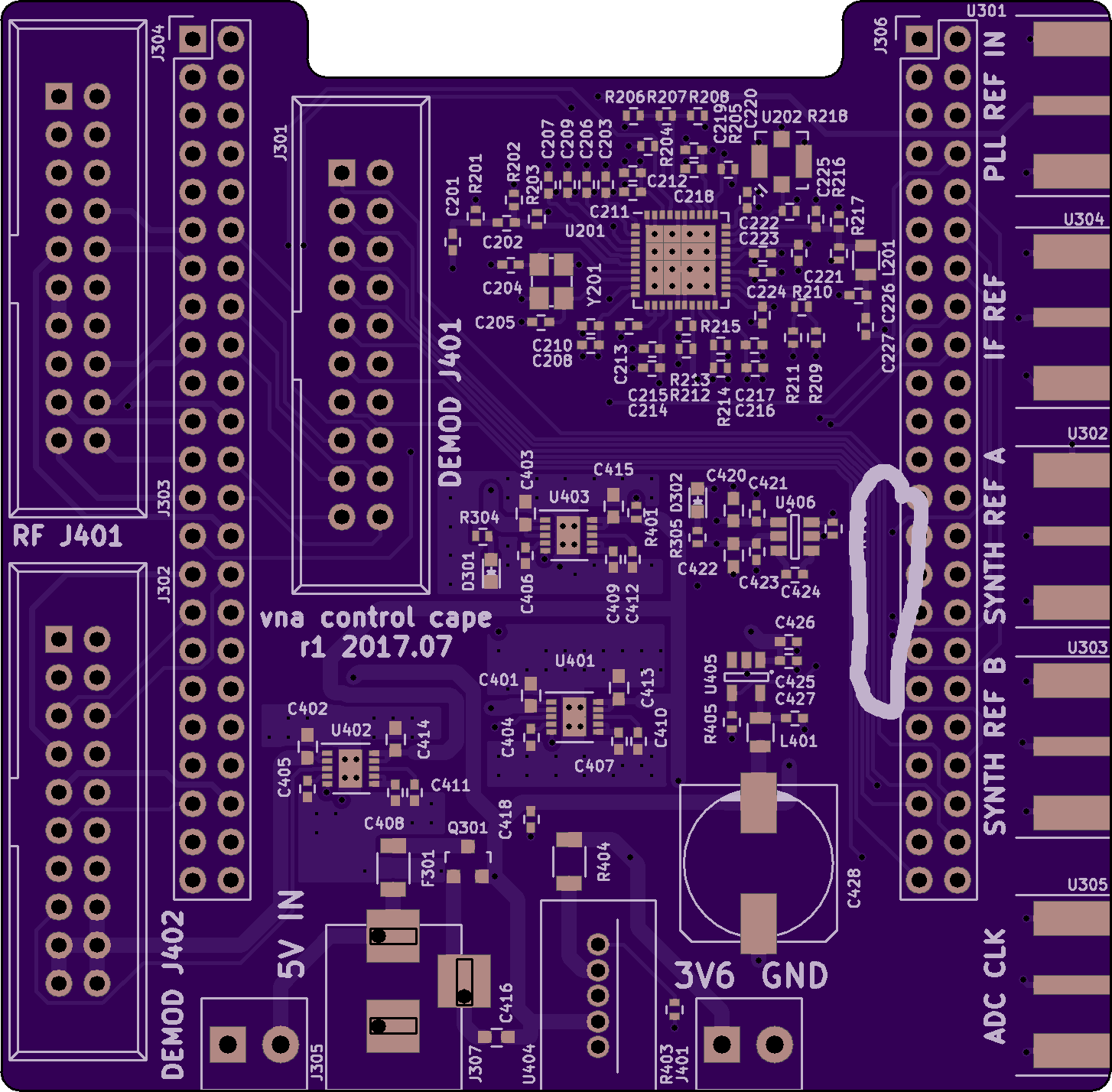
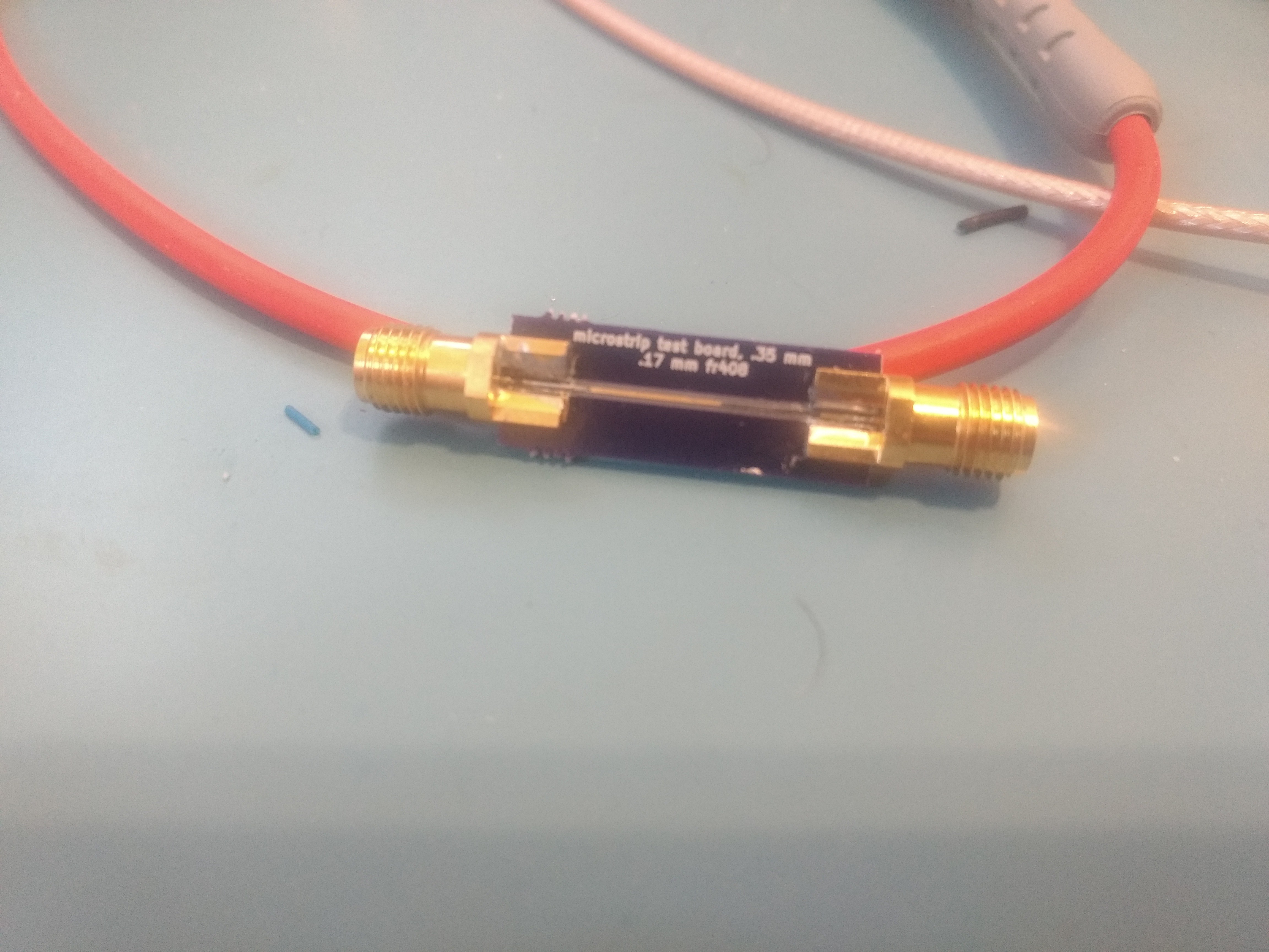
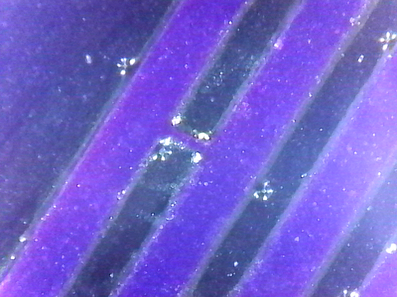 At 250x magnification I spotted a 1 mil thick bridge between the two signal lines. Once I knew exactly where to look I backed off on the magnification:
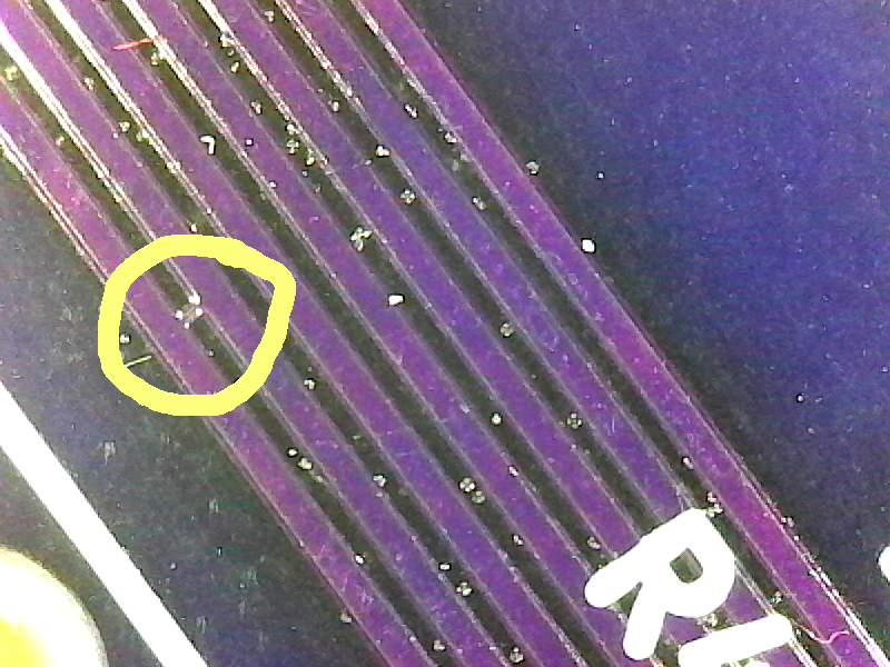


 drewrisinger
 P
P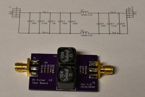
 Bharbour
Quite interesting project. Thumbs up!
Hope to have further continuing details..
Analog Devices introduced ADL 5960 frontend for low cost VNA( up to 20GHz freq.) Oct. 2021, which seems also quite promising.