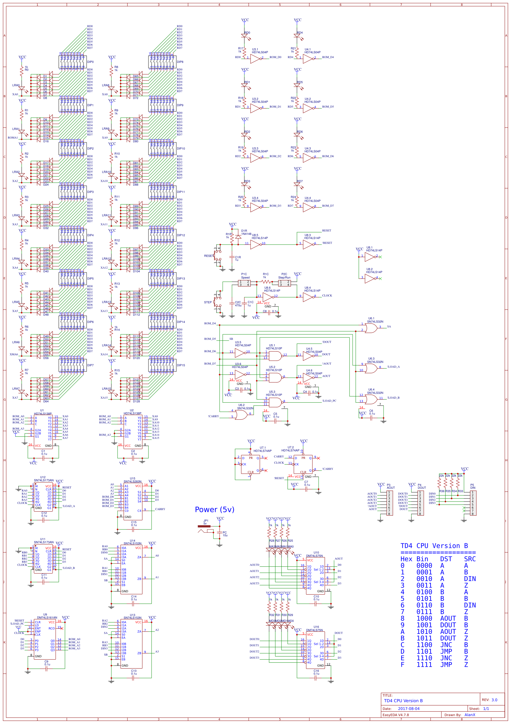
 agp.cooper
TD4 CPU
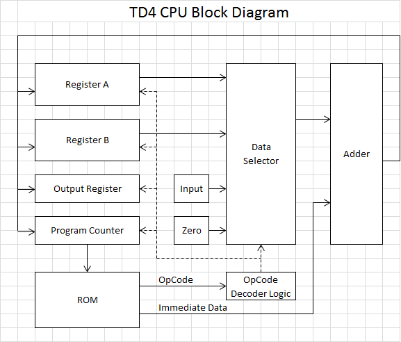
Here is a schematic from the Internet:

(source: http://kamakurium.com/wp-content/uploads/2016/01/cpu_td4.jpg)
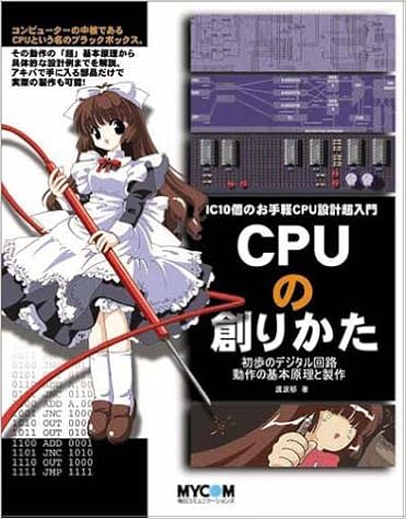
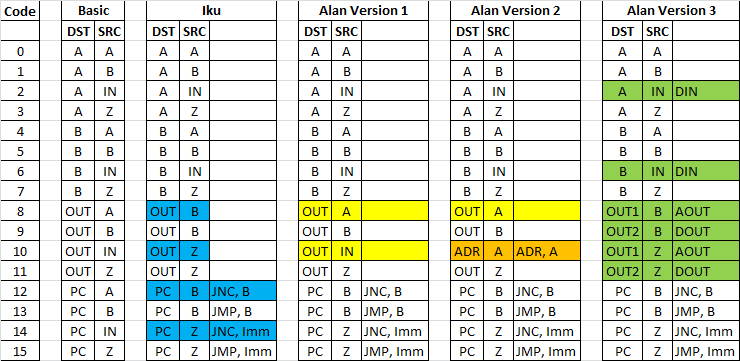
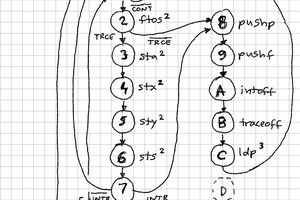
The entire CPU has only 12 TTL chips. Yes it has a switch based ROM! The schematic also shows the 12 OpCodes. It is not perfect, you cannot add the two main registers together and it cannot access any RAM. The author is Iku Watanabe, his book is available from Amazon but it is in Japanese:
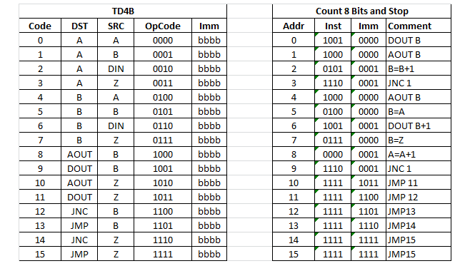
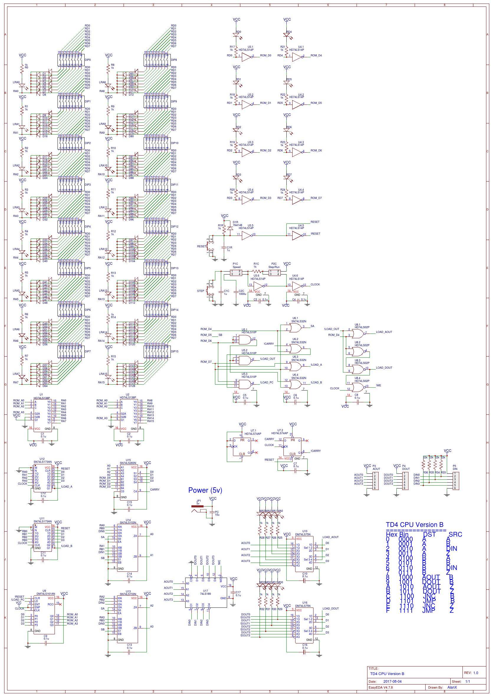
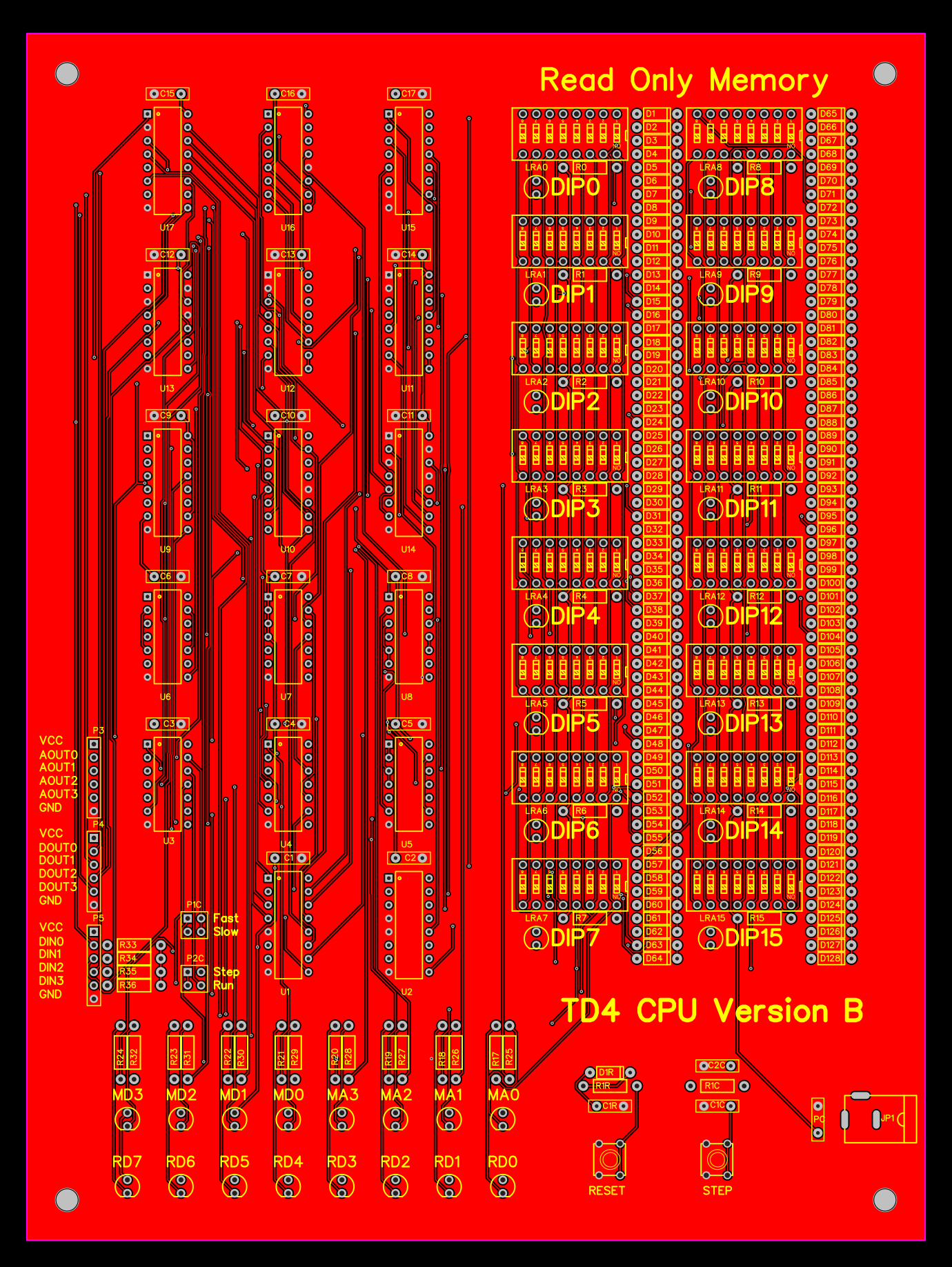
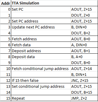
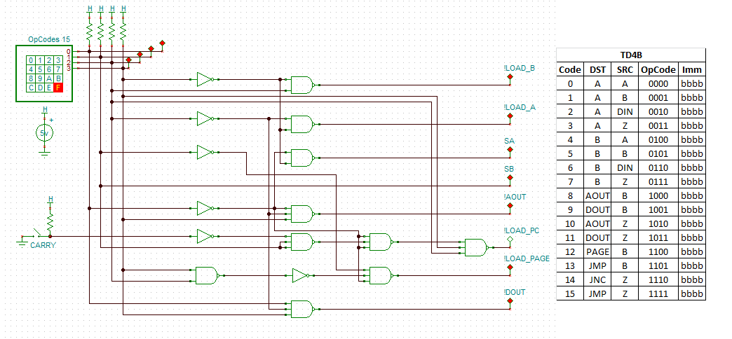
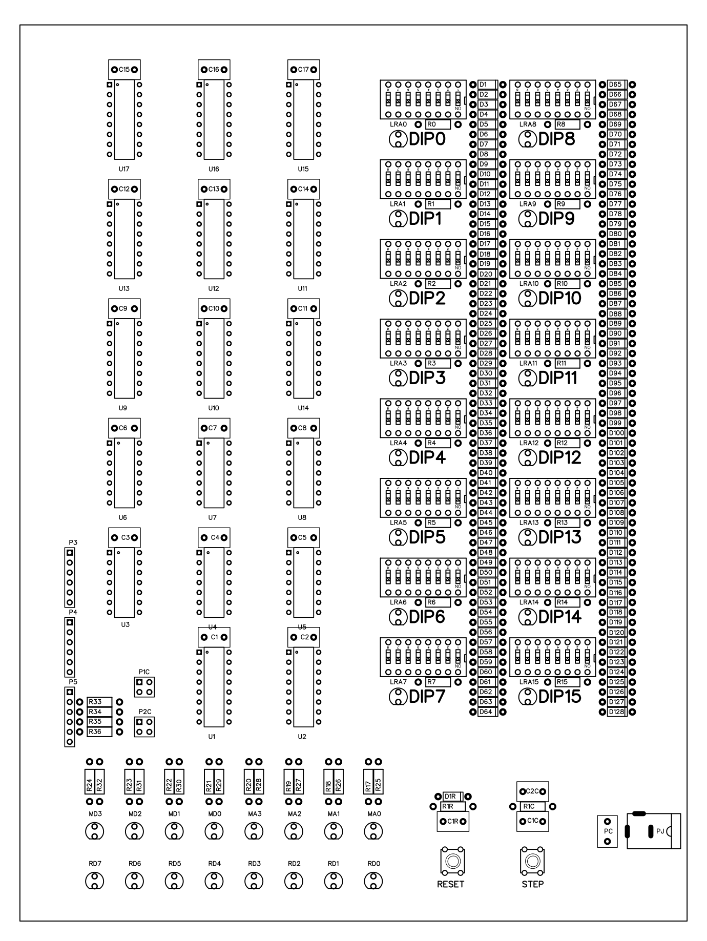
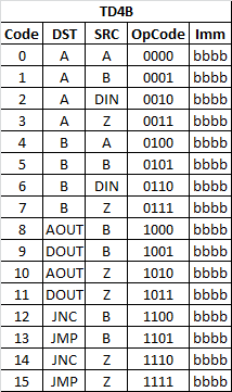
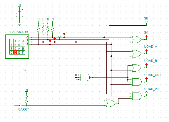
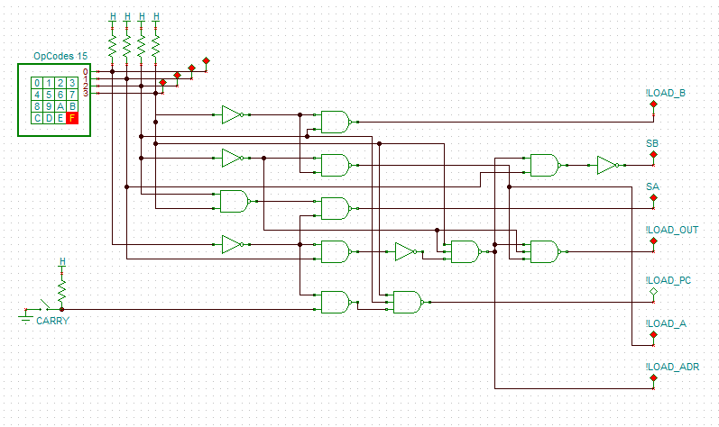
I like most of the design but I want to map the full 16 OpCodes and make room for an address register. Yes I want to access some RAM.
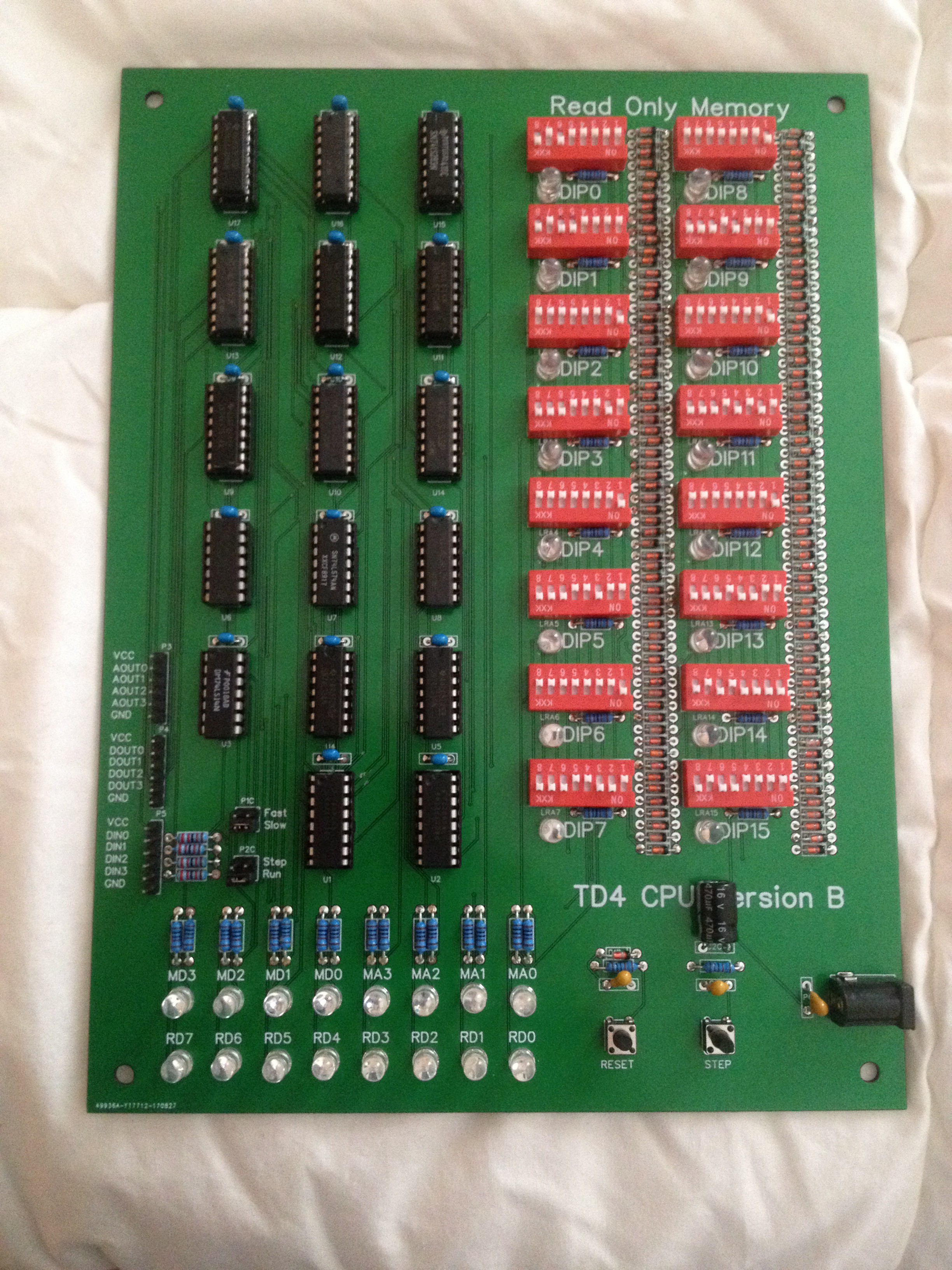
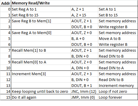
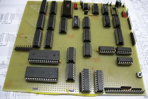
Flashing LEDs
Most of the units have lots of LEDs that really add to the special effects when it is running:

(source: http://img.makebooth.com/b21065f903ae8f138b1b21cd28bcbef5,jpeg)
One guy even build a relay version:

(source: http://www.geocities.jp/team_zero_three/TD4/td4r_ldb_imm_.jpg)
AlanX


 zpekic
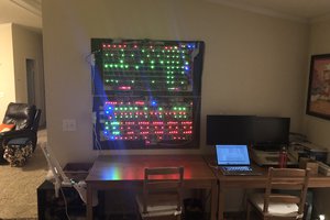
 spudfishScott
 jaromir.sukuba
Yea the clock and reset lines are swapped, a correction on that would be nice.