 Keith
Keith68B09E or 63C09E running at 2 MHz
120ns 32K EEPROM
100ns 32K SRAM
Already have an account? Log in.
To make the experience fit your profile, pick a username and tell us what interests you.
68B09E or 63C09E running at 2 MHz
120ns 32K EEPROM
100ns 32K SRAM
J070-U11_EQN.txtInitial analysis, NOT TESTED!plain - 1.69 kB - 05/28/2022 at 16:18 |
|
|
J070-U10_EQN.txtInitial analysis, NOT TESTED!plain - 2.36 kB - 05/28/2022 at 16:18 |
|
|
J070-U9_EQN.txtInitial analysis, NOT TESTED!plain - 1.41 kB - 05/28/2022 at 16:18 |
|
|
J070-U11-EQN.txtoutput from jed2eqnplain - 887.00 bytes - 05/28/2022 at 16:17 |
|
|
J070-U10-EQN.txtoutput from jed2eqnplain - 1.11 kB - 05/28/2022 at 16:17 |
|
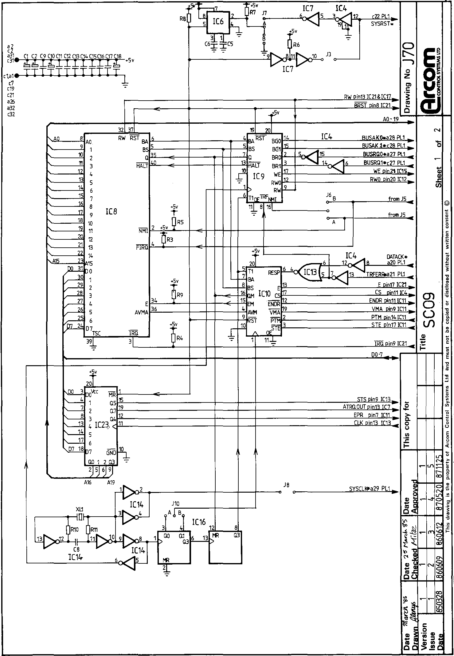
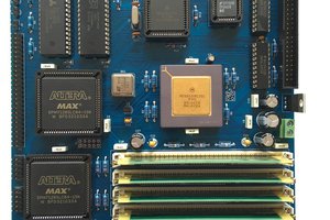
We start by looking at the Arcom SC09 board, see Figure 6.26(a). IC8 is the 680B09E processor and its E and Q clocks are produced by PAL IC10.
However, since the data could take some time arriving when an STEbus access is performed, the E and Q clocks are stopped during the STEbus access, thus ‘halting’ the 6809. IC10 waits for RESP to go LO (DATACK* or TRFERR* asserted) before releasing the processor from its stopped state. The maximum amount of time a 6809 can have its clocks stopped is 10 µs if it is left longer than this it can lose the contents of its internal registers. To prevent this happening IC16, a counter, drives Q3 HI after 8 µs, and when IC10 sees Q3 go HI it restarts the clocks. The timeout signal is also sent to IC9, another PAL, which triggers the 6809’s /NMI line, thus informing the processor that a timeout has occurred. A timeout can occur for two reasons: either a slave malfunctions and doesn’t assert DATACK* or the 6809 accesses an STEbus location where there is no slave.
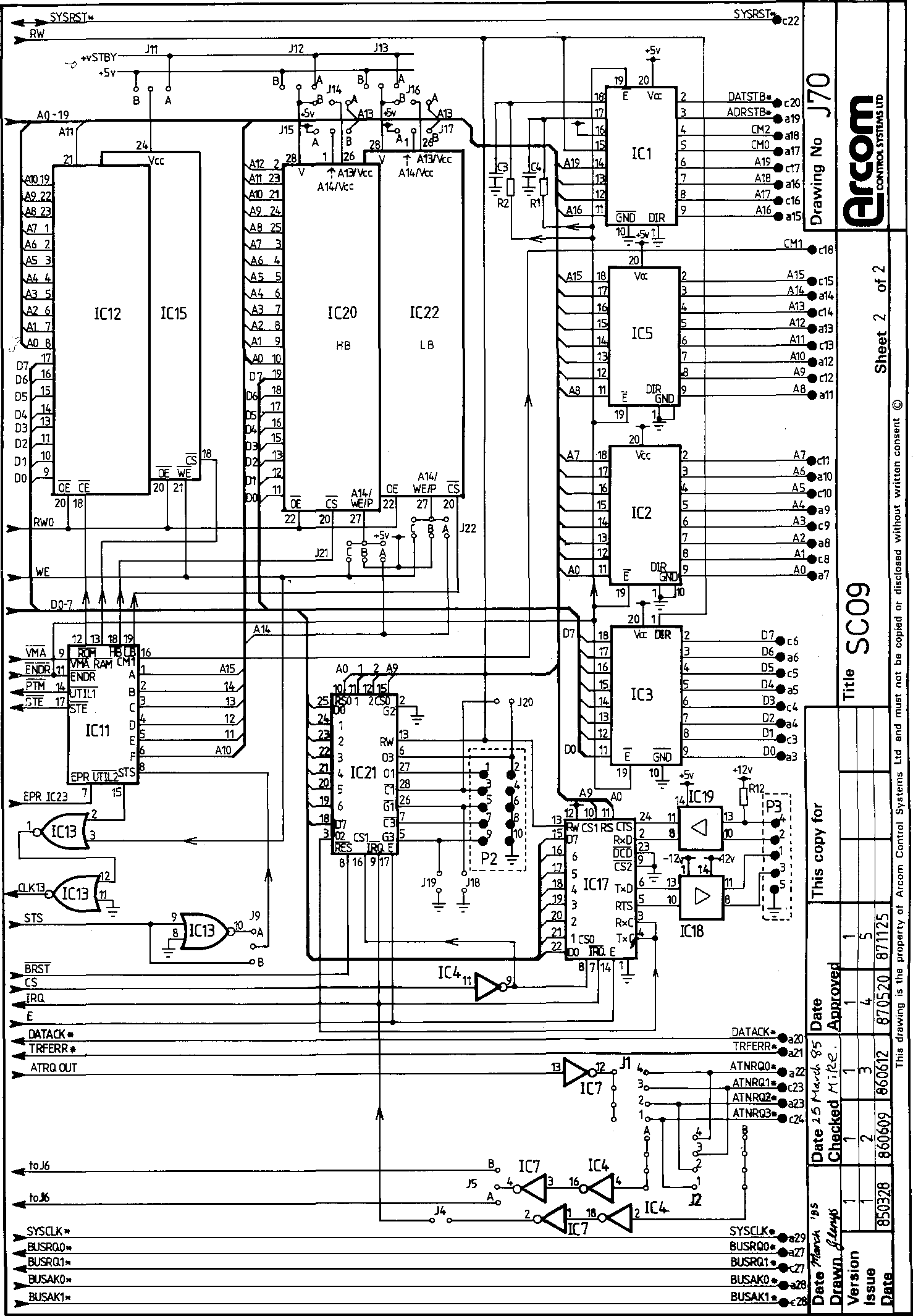
Passing on to Figure 6.26(b) of the circuit diagram, we notice four memory chips. IC12 is a 4K EPROM located at the top of memory, IC15 a 2K (6116) static RAM chip. The sizes of these chips would now be classed as small, but they are indicative of the date of design (1985). ICs 20 and 22 are RAM or EPROM chips (size 8K to 16K). IC11 is the memory map decoder PAL (16L8). This PAL also maps STEbus I/O locations into 6809 memory space - if a certain region of memory is accessed then the SC09 performs an STEbus cycle with CM1 LO (an I/O cycle). IC21 is a PTM (Programmable Timer Module, 6840), and IC17 is an ACIA (Asynchronous Communications Interface Adapter, 6850) or UART. ICs 18 and 19 drive and receive the RS-232 lines to and from the ACIA.
IC23 is a latch which stores the top four address lines, A16-19, for STEbus accesses, thereby extending the 6809’s address space from 64K to 1Mb. The latch also contains two control bits (EPR and STS) which modify the SC09’s memory map when set or cleared.
ICs 1, 2, 3 and 5 buffer data and address bus signals onto the STEbus. The buffers are enabled by the ENDR signal from IC10. ADRSTB* and DATSTB* are just this signal delayed by a resistor and capacitor to give the minimum 35 ns setup time required by the STEbus spec.
PAL IC9 contains the STEbus arbiter: BUSRQ0, 1* come in and cause IC9 to assert the 6809’s /HALT signal. When the 6809 has halted, as indicated by its BA and BS status signals, IC9 grants the STEbus to the appropriate requester. Notice that this means that the SC09 always acts in the default master mode and assumes it has control of the bus when it is running.
Figure 6.26a The SC09, a 6809 STEbus CPU board.
Figure 6.26b The SC09, sheet 2.
The designer told me that this board was far harder to design than more advanced processors like the 68020. It stretches the clocks for various reasons:
The Motorola 68B09E is an NMOS device and a dynamic design, so the clocks cannot be stretched beyond 10μs. So this board limits STEbus accesses with a timeout of about 8 microseconds.
The Hitachi 63C09E is a CMOS device, but also dynamic. The minimum clock rate is 0.5 MHz, so the clocks cannot be stretched beyond 2 μs if this CPU chip is fitted.
The I/O chips need a fixed clock rate (E) to generate baud rate clocks and general timing. This board solves this problem by having separate clocks for the CPU and the I/O chips. The board stretches the CPU clock to synchronise with the I/O clock when accessing I/O chips.
2019-05-30
I'd been putting this project off for a while because it is very complicated to get fully working and I have no known-good firmware specifically for it. I considered porting a monitor but a BASIC interpreter would be more impressive. Grant Searle's minimalist 6809 design has Microsoft BASIC and the same 6850 ACIA serial chip. I would still need to reassemble the firmware source code with different addresses for this chip.
Grant's source code uses Motorola style. Comments begin with an asterisk instead of a semicolon, or not at all if there is enough for the assembler to make valid instruction bytes already.
The assembler I use (https://www.asm80.com) uses the most common syntax it can for all processors. So I had to do a lot of editing to get it to assemble, and it is still not generating a hexfile identical to the one from Grant's site.
It occurred to me that I could program the GAL chips to put the memory map the same at Grant's design. I can then use Grant's ROM unmodified. Also, I don't have to get everything working at once. Just the CPU and serial port at first. Then the STEbus, which requires cycle stretching. The tricky bit is getting it back in sync with the ACIA and PTM chips, which require fixed cycle times.
If that proves too difficult for me then I may replace them with chips that have independent clocks, such as a real-time clock that can interrupt the CPU every second (for OS/9 and Flex operating systems), and the Zilog SCC which is a far more powerful serial chip.
Finally, I might also replace the serial chip with a USB module from FTDI. These have a really simple FIFO-like interface, and avoid the need for external RS323 to USB converter cables.
2019-05-31
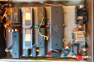
Inserting jumper links, I notice the manual and circuit diagram are both version 1 issue 5, applying to version 1 issue 2 boards. I have a version 1 issue 1 board, lacking link areas J21 and J22. I can work around the differences.
2019-06-01
Finished porting Grant's code to use the online assembler syntax. Found one error, and other errors due to operator precedence which were fixed by brackets. Original source was all upper case, which make sense if the host machine only has upper case e.g. the 6809 CoCo and Dragon.
2019-06-02
Had a look at some other 6809 machines to see what their memory maps look like. E.g. the CoCo, Dragon, and Acorn 6809 card. Looks like operating systems really need a counter/timer to interrupt them at least once per second. The CoCo and Dragon don't have this but seem to manage without. The Arcom SC09 has a 6850 programmable timer module. The Acorn 6809 card has a 6522 which can generate interrupts and as a bonus provide parallel I/O for driving a printer.
I think a proper real-time clock would be better, providing interrupts and a useful clock/calendar.
2019-06-20
Stage 1, first attempt at programmable logic tried. E and Q signals running at a quarter of master clock - correct. Address, data and control signals flapping away, indicating the CPU is running even if it is garbage. Nothing coming out the serial port, because the Timer chip needs to programming to drive the Tx/RX clock of the ACIA chip. Grant clocks his ACIA from the E signal, at 1.8432 MHz. My board has a 16 MHz crystal and 2 MHz E signal. I need either a separate baud rate clock or change the 16 MHz master crystal to a 14.7456 MHz crystal.
2019-06-21
14.7456 MHz crystal fitted. 6840 timer chip removed and E wired to TX/RX clock pins. Still no sign-on message. Looks like I need to get the logic analyser out to see what the signals are actually doing.
2019-06-26
Logic probe showed the TX line was not valid TTL voltage. It was 0.9 volts. Dead buffer? Removed buffer, it raised to 5V. Replaced buffer, still 5V. Had it been in the wrong way round? Check the photo, yes it had. And my +/-12 source was dead.
2019-06-28
Read and Write signals modified. Memory system runs in "early write" mode, R/!W lines set up before data...
Read more »


It is. I have that book, though the PAL equations are not given there.
 Tobias Rathje
 Colin Maykish
The SC09 board is apparently the reference platform described in the book "
Microprocessor System Design: A Practical Introduction" By Michael J. Spinks (1992).