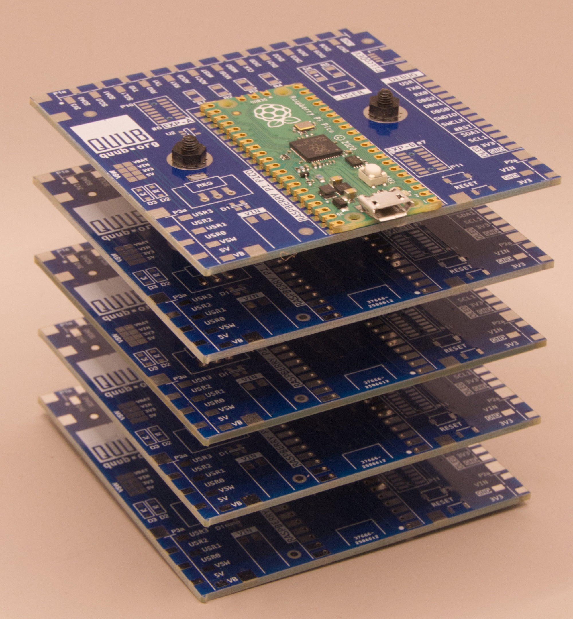
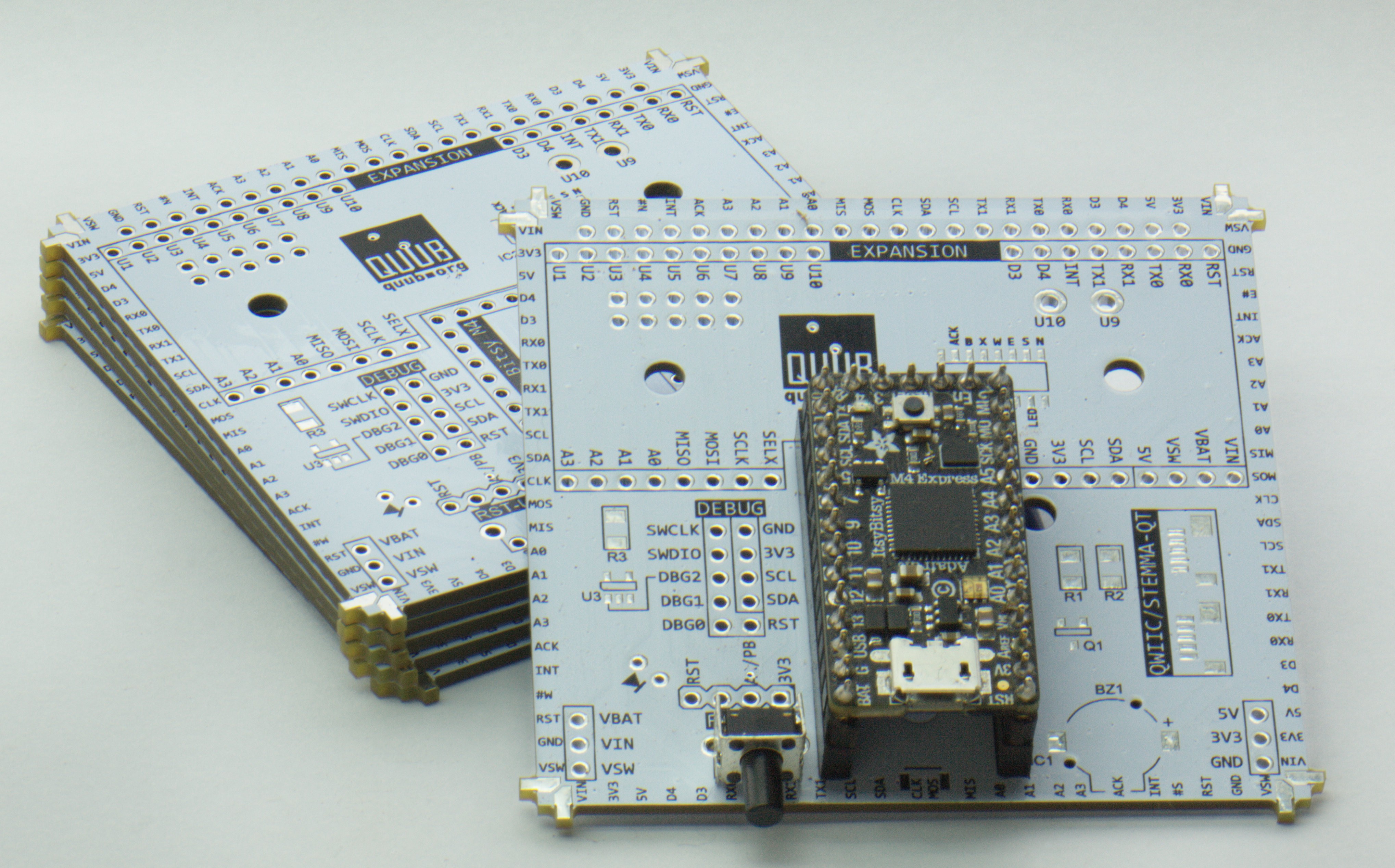
Close
0%
0%

The Quub

Open-source microcontroller system based on an Raspberry Pi Pico core processor and stackable interface boards

robrob
Public Chat
Similar projects worth following
Open-source microcontroller system based on an Adafruit Itsy Bitsy core processor and stackable interface boards

This is a new version of an old idea that I've been playing with for years, and I mean literally for years.

Overall the delay has been good though in many ways as the current design is way better than early ones were.

There is a rudimentary website hosted as a sub domain on my main site here

quub.org

QUUB is an open-source, micro controller system based on a core processor, addressable daughter boards, and remote IO modules. It is a general-purpose embedded microprocessor system, the form factor is based on a main MCU board and multiple stacked IO boards called "stackables". It can therefore accommodate designs from the simplest flashing-LED project to a complex multi-processor robot controller.

The QUUB system has the following features.

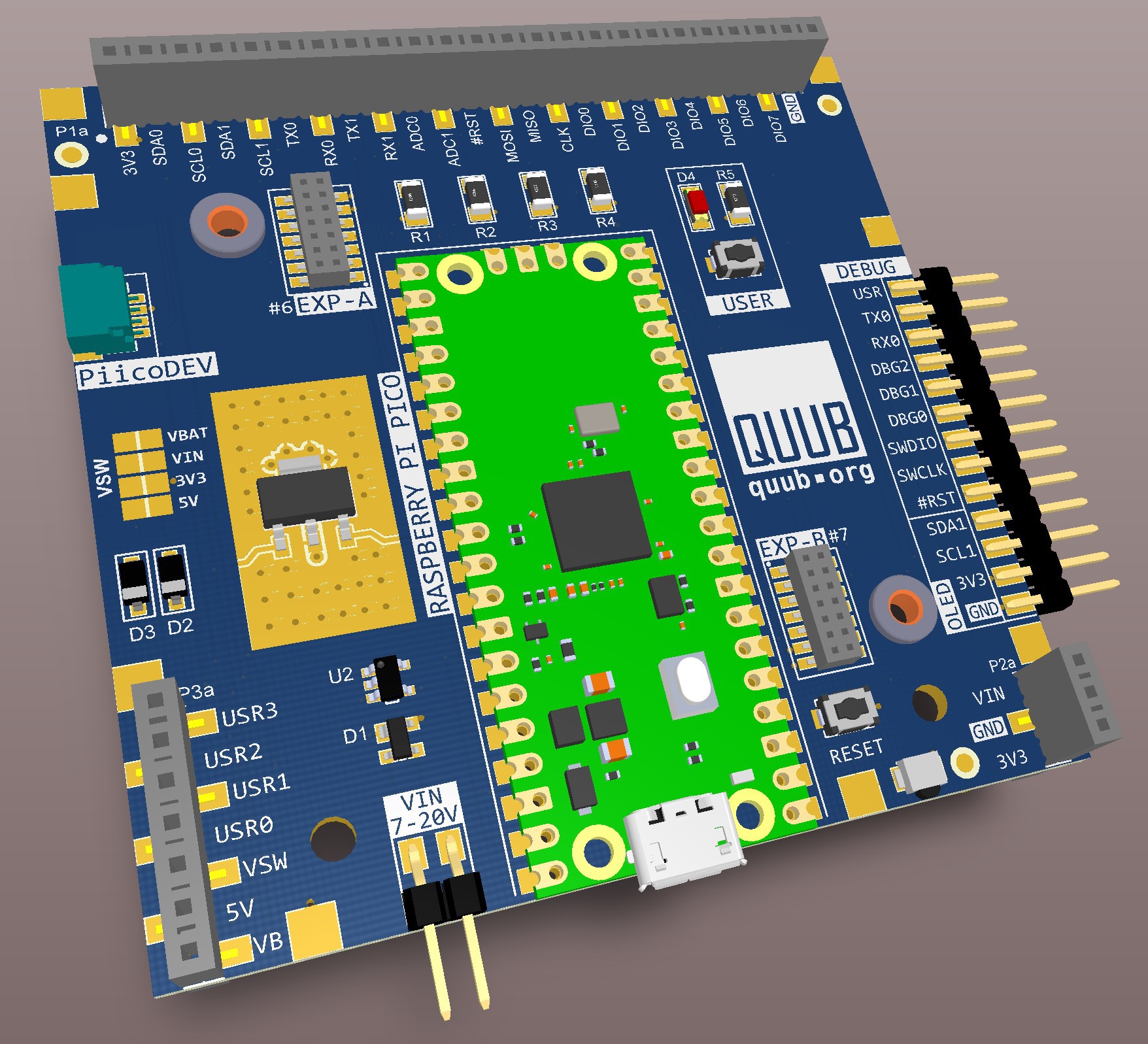
  • The core processor board is an Raspberry Pi Pico module, this is a dual core 32-bit Cortex M0+ processor running at 133MHz.
  • Small form factor, nominally 70 x 70mm (2 3/4 x 2 3/4 inches).
  • A unique method of attaching four "sides" (vertical PCBs). These sides make the QUUB design "self enclosing", no need for a box.
  • Addressable daughter boards can be stacked above or below the core processor.
  • Two optional "mezzanine" expansion modules with a 14-way interface, useful for small addons such as an SD card socket.
  • 24+3+7-way "stackplane" using stackable headers.
  • The stackplane has provision for all power signals, 2x I2C, SPI, 2x UART, 2x analogue in, 8x digital IO, four user-defined signals, and optional addressing of daughter boards.
  • Up to 8 daughter boards can be addressed and can therefore share the same system IO lines.
  • A PiicoDEV (STEMMA-QT/QWIIC) header.
  • Dedicated debugging pins as well as the standard SWD interface brought out to a header.
  • Debugging connector directly compatible with a standard .91" OLED display that can be used for general IO or debugging.
  • Front-panel accessible pushbutton that can be used for reset, designed to be activated through a small hole in the PCB.
  • 7-20 volt polarity-protected VIN.
  • One switched power signal that can be used by the MCU to shut down peripherals such as a GPS or wireless transmitter.
  • Two mounting holes suitable for an M3 bolt or similar-sized screw.

If you need a system with over 20 analogue inputs, or maybe 30 serial ports, or more than 200 digital IO connections, no problems, QUUB can do that and more.

Stackplane (backplane for the QUUB stack) The stackplane consists of three headers of 24, 7 and 3 connections. With the vast array of I2C and SPI peripheral IO chips now available it makes sense for larger and more complex applications to have a backplane with just a few signals that communicate with slave devices using one of these popular serial interfaces. However for tinkering or simpler applications the QUUB can be used like any of the other development boards available.

There are four user-defined signals on the stackplane, these signals pass up the entire stack and can be used by any stackable for whatever purposes. One example would be a power supply stackable sitting at the bottom of the stack that needs an ON/OFF switch and a power indicator LED at the top of the stack.

Side panels (sides) Provision is made to solder small PCBs at right angles to the main PCB. These can be used to enclose the board so a box is not normally required. If all stackables implement these side panels the QUUB stack becomes fully enclosed on the bottom and sides. This leave the top.

Lids Lids are special stackables that are only used on the top of the stack. They are 3mm larger than the standard stackable size so they cover the stackable sides below them. Lids can be blank and used simply to fully enclose the stack, or they can also have active circuitry, such as an LCD display and some switches to provide a simple user interface to the stack's application.

Bases A base is not normally required as the MCU board has no components on the solder side of the board. However the MCU may not be the lowest stackable and the one that is may have through-hole components. In this case a base board may be required to isolate the electronics from whatever the stack is placed on.

Another reason to have a base board is to accommodate large components, for example a board that has four relays and a 100A shunt, these will not fit on the standard stackable PCB size...

Read more »

211125__MG_9886.jpg

Latest PCBs for the CPU.

JPEG Image - 1.69 MB - 03/16/2022 at 23:29

Preview
Download

Schematic.pdf

Schematic design as at 13 Sep 2021

Adobe Portable Document Format - 108.72 kB - 09/13/2021 at 10:16

Preview
Download

7-01-2021 6-29-47 AM.jpg

This is the new design. Where as the original only had a single solder-on side this has four, all of which can house electronics and/or be connectors for IO interfaces.

JPEG Image - 391.94 kB - 01/06/2021 at 20:44

Preview
Download

  • Slight update

    rob02/25/2024 at 21:56 0 comments

    Almost as soon as I received the last PCBs I had a few ideas for some changes. So I'll be getting new ones made and won't be using the last ones. They cost almost nothing to make these days so might as well get it as right as possible eh?

  • Yet another processor and PCB design

    rob02/20/2024 at 05:22 0 comments

    This project started about 10 years ago and has had more starts than Phar Lap (Aussie joke). Yet more processor PCBs made recently. The core processor has been changed to a Raspberry Pi Pico, partly because it has castellated pads so it can be soldered directly to the QUUB board, and partly because I think that there is a much larger following and body of work out there for that particular processor.

    Here are five of them stacked, giving some idea of where the QUUB name came from :grin: Of course one would not stack five MCU boards, I just wanted to check the mechanical aspects of the idea.

  • New PCBs received.

    rob03/16/2022 at 23:39 0 comments

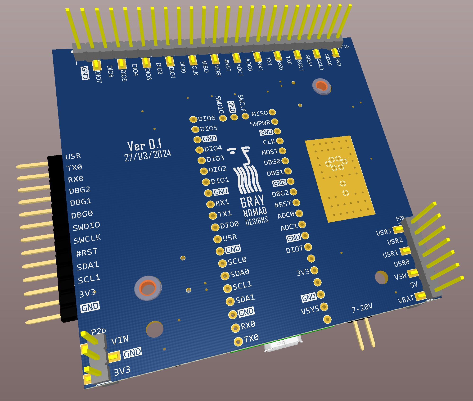
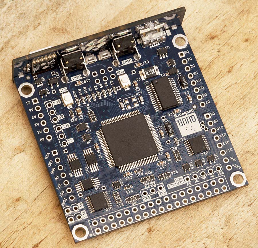
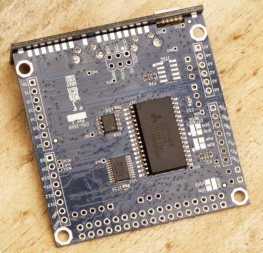
    The new CPU boards are here, I already have some changes in mind so I may not even test these one, we'll see.

  • A quick video showing most of the QUUB features.

    rob10/14/2021 at 21:38 0 comments

  • PCB v2 is almost ready for fab

    rob09/13/2021 at 07:07 0 comments

    The PCB v1 has been in use for a while now and some support code has been written to remap a few of the default Adafruit pins to get a second UART etc.

    During the course of this I had many new ideas and have modified the PCB substantially. It's almost ready to be fabbed as v2 now, here's a 3D render of the new look.

    NOTE: Circuit boards called "walls" can be soldered at right angles to the main PCB on the four edges, these have access to all the backplane signals so can have active electronics and connecters to facilitate IO, or just be blank to form the sides of a box. These walls are designated as per the cardinal points of a compass, N, E, W, and S.

    With all four walls in place and the addition of a top PCB the design is essentially "self enclosing".

    The "stackplane" is now three Arduino-style socket strips, one is 22-way with most of the logic signals and two are 3-way that mostly carry power.

    The expansion bus has been extended to include most of the backplane signals. The expansion module now sits at the same height as the Adafruilt CPU module. Normally this expansion module would be used for small functions that don't justify an entire stackable daughter board, such as an RTC or micro SD card. It could also be used for IO like a serial port or more STEMMA-QT/QWIIC interfaces as it has some access to the west and east walls and even the south wall if it is designed in an L shape.

    There is now hardware decoding for six slave select signals, one for each wall, one for the expansion module, and another for the backplane. Thus up to six devices can share signals such as the SPI interface. Alternatively up to 16 stackable and addressable boards are allowed for and each such board can provide a vectored interrupt with a protocol for this being largely defined.

    Two STEMMA-QT/QWIIC connecters have been added, this is fast becoming a standard so it makes sense to include them. I always planned to have a quad buffered interface for this and still will, but these two connecters allow the use of STEMMA-QT/QWIIC modules right off the bat.

    Another addition is dedicated pins on the debug header, these can be used as scope triggers or for other high-speed measuring. Also internal data variables can be bit banged out these pins and read on a scope. Code has been written to do this. Naturally a standard ICE debugger for an ARM can be used as well and I have plans to design a debug board with some useful features.

    Finally both the debug and expansion headers allow for the direct plugging in of a common 0.91" OLED I2C serial display, either for debugging or general UI purposes.

  • PCB fab is in progress

    rob06/25/2021 at 22:39 0 comments

    The design files have just been uploaded to JLCBPCB, this is the base board to hold the Adafruit CPU module. The tabs on each corner are to locate the side "walls" that can house more circuitry and/or physical IO connectors.

  • A new simpler and more powerful design

    rob01/06/2021 at 20:58 0 comments

    This is the new design. After a few years of inaction I've come up with a modified design that is much simpler and yet more powerful in most ways.

    The original design only had a single solder-on side, this new design has four, all of which can house electronics and/or connectors for IO interfaces.

    Another big change is the processor. Despite the fact that I love their chips and tool chain, after total lack of support from NXP I've gone with an off-the-shelf design in the form of a tiny carrier board with a ATSAMD51 Cortex M4. This is an Adafruit product that has good support and is Arduino ready. Therefore I will spend almost no time debugging the processor electronics and fighting with the development toolchain only to wind up with something that nobody will want to use because it's not "Arduino inside".

    Of course, as the processor is on a carrier board, and the backplane is very generic, a new processor version can be designed at any time and just plugged in.

  • New version being considered

    rob09/09/2019 at 01:00 0 comments

    This project has languished for a long time but I think I will resurrect it. 

    The format will change but still be similar in many ways, with stackable boards and solder-on front panels. The main difference is that the new design uses an LPC1549 ARM processor and has built in RS485 networking using a protocol I am designing called R3N (Robust Redundant Ring Network).

    Why bother when you can run Linux and WiFi or Ethernet on a board 1" square these days? I dunno, I just like doing this stuff and I can see uses for it.

  • Boards back from PCBA

    rob09/24/2014 at 21:55 0 comments

  • PCB and PCBA in progress

    rob05/06/2014 at 23:29 0 comments

    The design files have been sent to a company in the UK, they wil fab the PCB and load four boards with components for use as prototypes.

View all 11 project logs

Enjoy this project?

Share

Discussions

rob wrote 03/09/2014 at 22:48 point
PCB design finished for the first core processor board, an ATmega2560 with 512k external SRAM. Getting PCBA quotes for first prototypes soon.

  Are you sure? yes | no

Similar Projects

Does this project spark your interest?

Become a member to follow this project and never miss any updates