 Bud Bennett
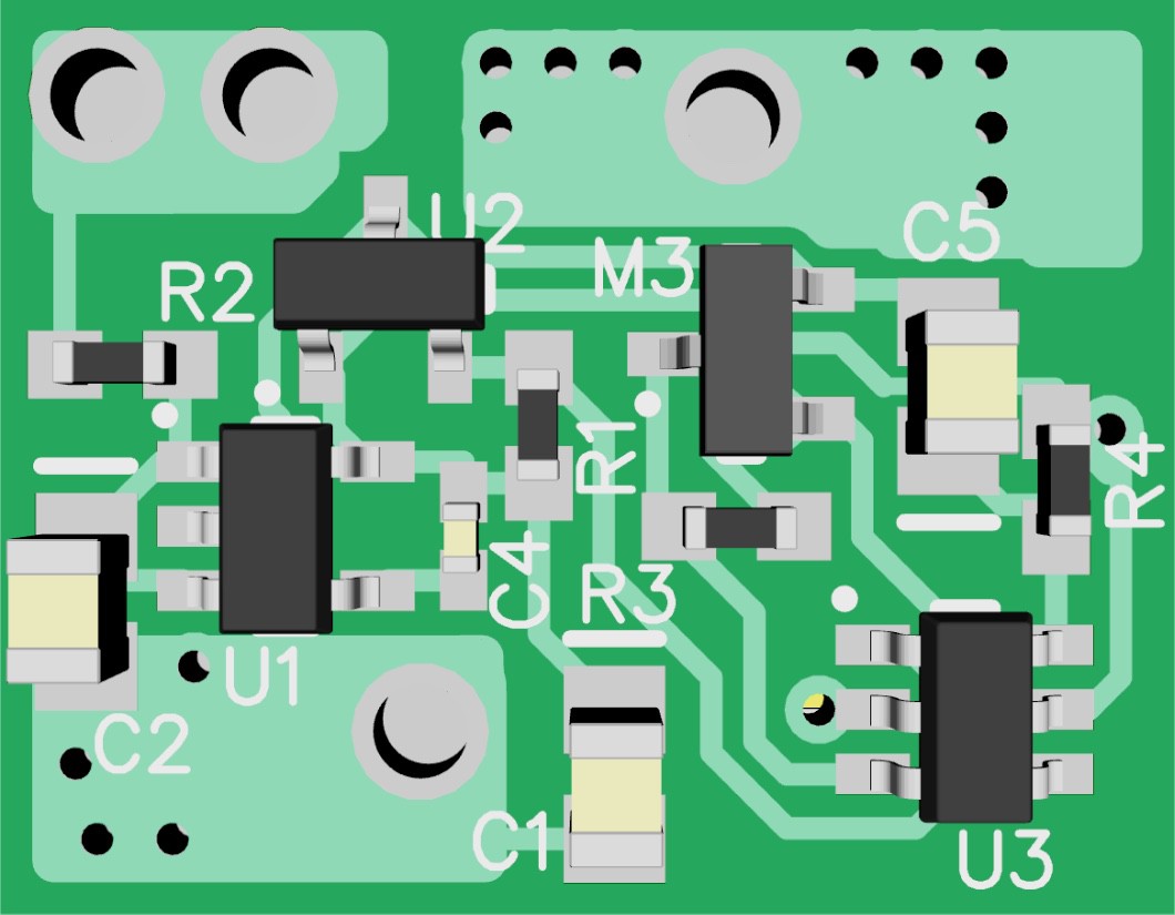
I am not a PCB designer. All of my experience has been Analog and Mixed-signal IC design. A lot of it translates pretty well, but some of it doesn't. Here's the top and bottom sides of the 30A mag switch circuit. There's a lot of stuff to be aware of.
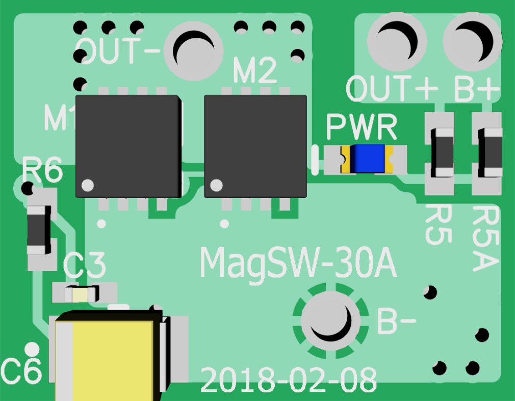
The bottom side (the first image above) is where all of the action is. You'll notice that the top quarter of the board is nearly empty, except for metal and pads. I had to overcome the fiction that all of the pads must be located at the edge of the board. This doesn't apply here. The name of the game is low trace resistance. Keeping distances short and traces wide is the overall goal.
I'm going to use 2oz. copper for these board going forward. The sheet resistivity of 2oz. copper is about 0.25mΩ/square. It doesn't matter if the square is 1µm x 1µm or 100mil x 100mil it will have the same resistance.
The critical paths in this circuit are B+ to OUT+, the drains of M1 & M2 to OUT-, and from B- to the sources of M1 & M2. The resistance between the B+ pad and the OUT+ pad is only 1/4 square, so the resistance is negligible.
Next, the drains of M1 & M2 are about 1/4 square (0.06mΩ) -- it's difficult to determine because of the geometry so I'm making a guess. Notice that I moved the pad from the outside edge to a position centered between the two big FETs. If the pad was at the edge, the resistance would be 1-2 squares instead. I left space at the top of the board for the 16AWG insulated wire to run from the pad past the edge of the board. I expect that the lead connected to OUT+ will run along the top side of the board and the OUT- lead will run along the bottom side. I don't want them running over any components for reliability concerns. Yes, this makes the PCB bigger, but...reliability.
I moved the B- pad closer to the sources of M1 & M2 for the same reason. I can eyeball the resistance between B- and the sources of M1& M2 at about 1/2 square (0.125mΩ). But it would be much lower if the pad was located between M1 & M2, and closer to them. I might place a surface pad at that location to see if there is any improvement in insertion loss. Note that the B- lead will run over the top or bottom side of the board where there are no components.
Calculate the total switch resistance:
The FETs: 0.9mΩ @ VGS = 4.5V for 2 FETs in parallel
Drain to OUT- : 0.06mΩ (1/4 sq.)
B- to M1 & M2 sources: 0.125mΩ (1/2 sq.)
B+ to OUT+: 0.06mΩ(1/4 sq.)
Total Switch Resistance = 0.9 + 0.06 + 0.125 + 0.06 = 1.15mΩ
Heat Dissipation:
The power dissipation of the board with a 30A load will be around 1.2W. To get rid of the heat the metal needs to be maximized. That's why there's metal extending past where it really does any good and there are metal pours on the top side of the board.
Discussions
Become a Hackaday.io Member
Create an account to leave a comment. Already have an account? Log In.