 Bud Bennett
I was almost ready to order a new set of PCBs this morning when I got a notice of Martin's comment. His suggestion to use the TPS70950 LDO regulator was a gift. I had searched all over Digikey (and the web) for a low Iq LDO, but nada. The TPS70950 is absolutely perfect for this application. The key features of this part is the high input voltage (30V), the quiescent current (1uA), and the no reverse current feature, all of which removed the blocking diode and the protection diode that I had to use with the MCP1702 LDO. The only downside is that it is a bit more expensive: $1.04/each vs. $0.51 for the MCP1702. I replaced both the MCP1702 and the LT1761 with the TPS70950.
Other Small Changes:
The LDO has a fixed output voltage of 5V. The other components will function over a range of 2.5V to 5.5V so I only really need the LDO to clamp the VDD voltage. The higher VDD voltage should yield a better RDSon from the NCH FETs and also lower power dissipation at full load current. I expect that this change and the layout improvements should yield switch resistance < 10mΩ (more than a 3mΩ improvement).
The new LDO requires slightly different input and output capacitor values to be stable. The range of input capacitor values is pretty large and I only have one capacitor in inventory that will do the job -- a 6.8µF X5R/25V/0805. The LDO is not stable with output capacitor values greater than 47µF, so I'm using a 22µF X5R/6.3V/0805 and will have to rely on R6 (TBD value) to decouple the big 220µF tantalum and keep the LDO stable.
Other circuit changes are the new symbol for the D-type flip flop, and R5 was increased to handle the expected higher input voltages. R5 is really a placeholder and can be modified after the new boards are received.
The new schematics are posted in the details section of this project.
Layout Changes:
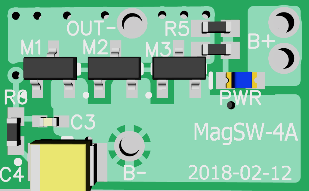
The biggest layout change to the 4A mag switch was that the OUT- pad was centered and moved closer to the drains of M1-M3. An additional 20mils were added to the height of the board to increase the width of the trace connecting all of the drains of M1-M3. The B- pad was moved very close to the sources of M1-M3 as well. These changes should remove 3-4mΩ of trace resistance.
I took care to make sure that the leads to the OUT-, OUT+, and B- pads don't cross over any components on the board. This is a reliability issue.
I'm hoping that this is the final second pass 4A board bottom-side layout:
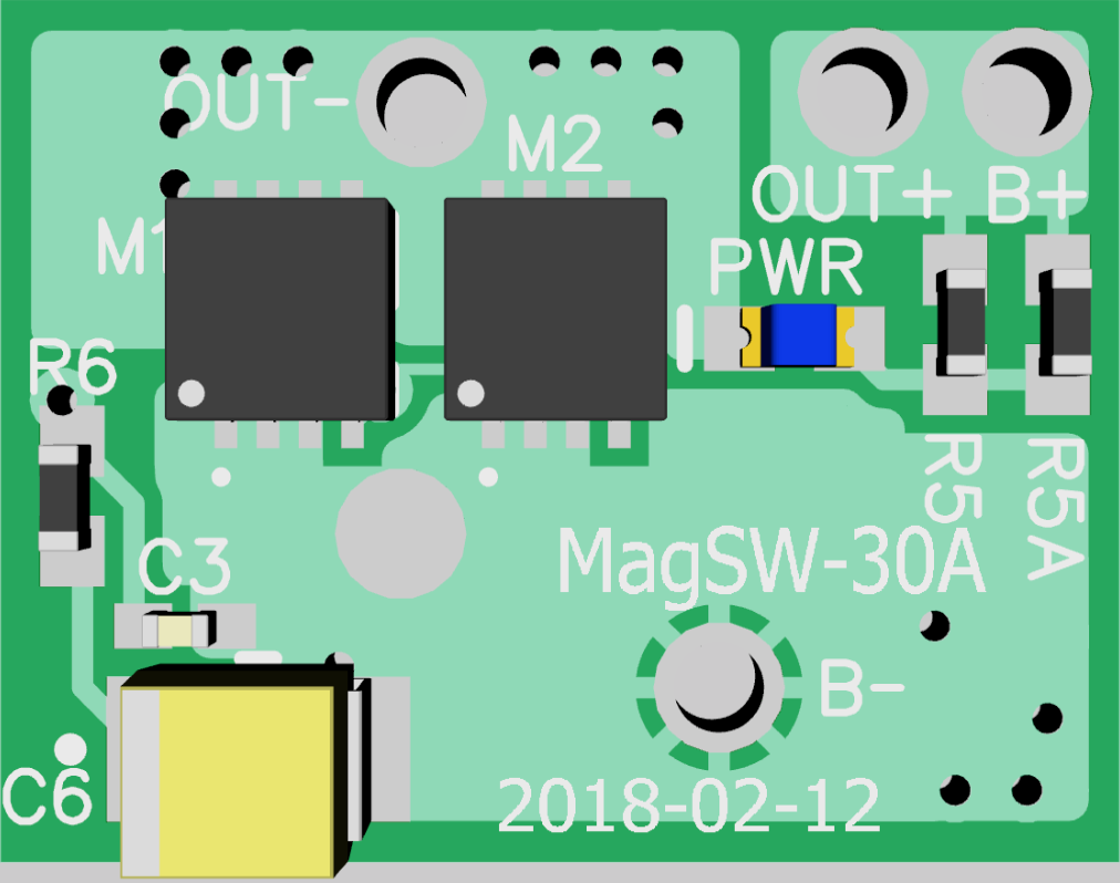
The 30A mag switch layout hasn't changed much from my "rumination" posting, but I did add a surface mount pad directly beneath the sources of M1 and M2 to see if that might improve the insertion loss:
Discussions
Become a Hackaday.io Member
Create an account to leave a comment. Already have an account? Log In.