 Anthony
The transistors I ordered arrived a bit earlier than I expected, so the next step is to prep/test the board. While transistors themselves have many more much 'interesting' properties (i.e. serving as amplifiers, etc), for our basic use case here we will be using them in their simplest form, as basically 'digital switches'.
First order of business then is to remove the solder mask from the top side of the board to get at the copper trace. There are also 'chemical' means of doing this, but unless you aim is to strip the entire surface of the board, after using the fiberglass pencil I would say there is no better way to do it.
'Before and After', revealing several traces:
A couple of points to note:
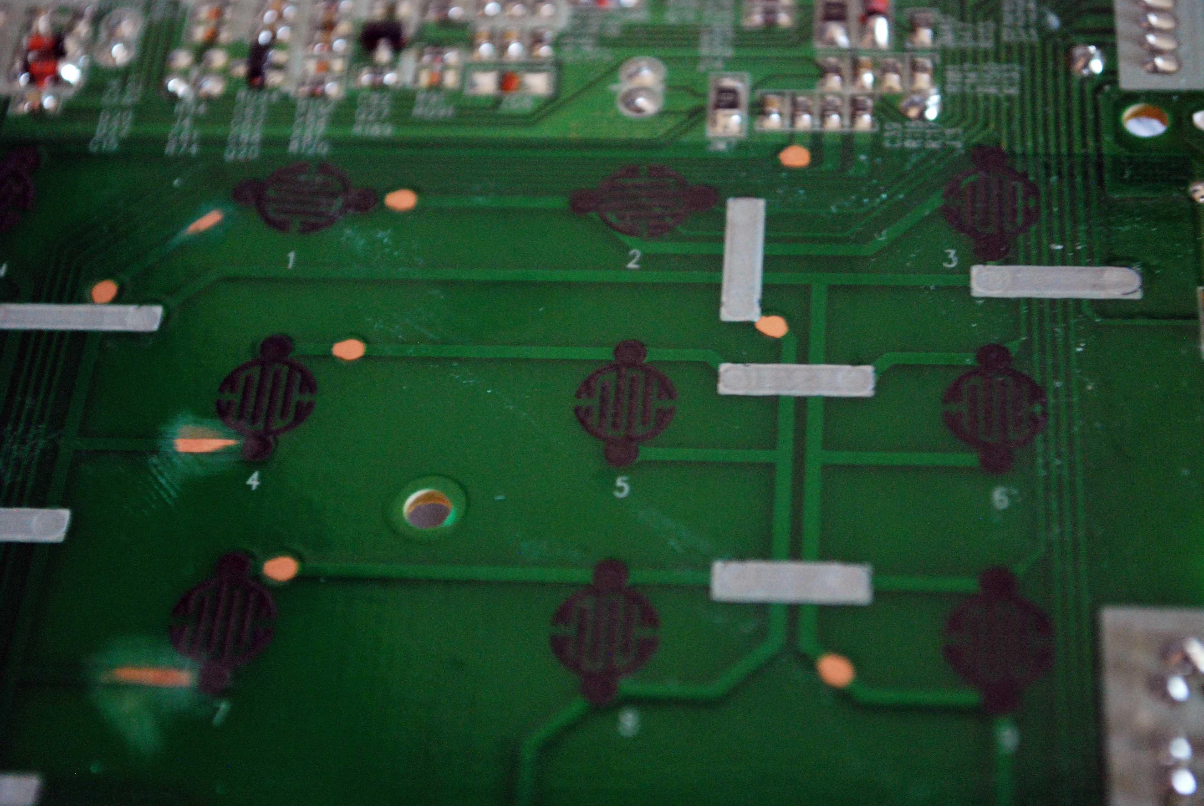
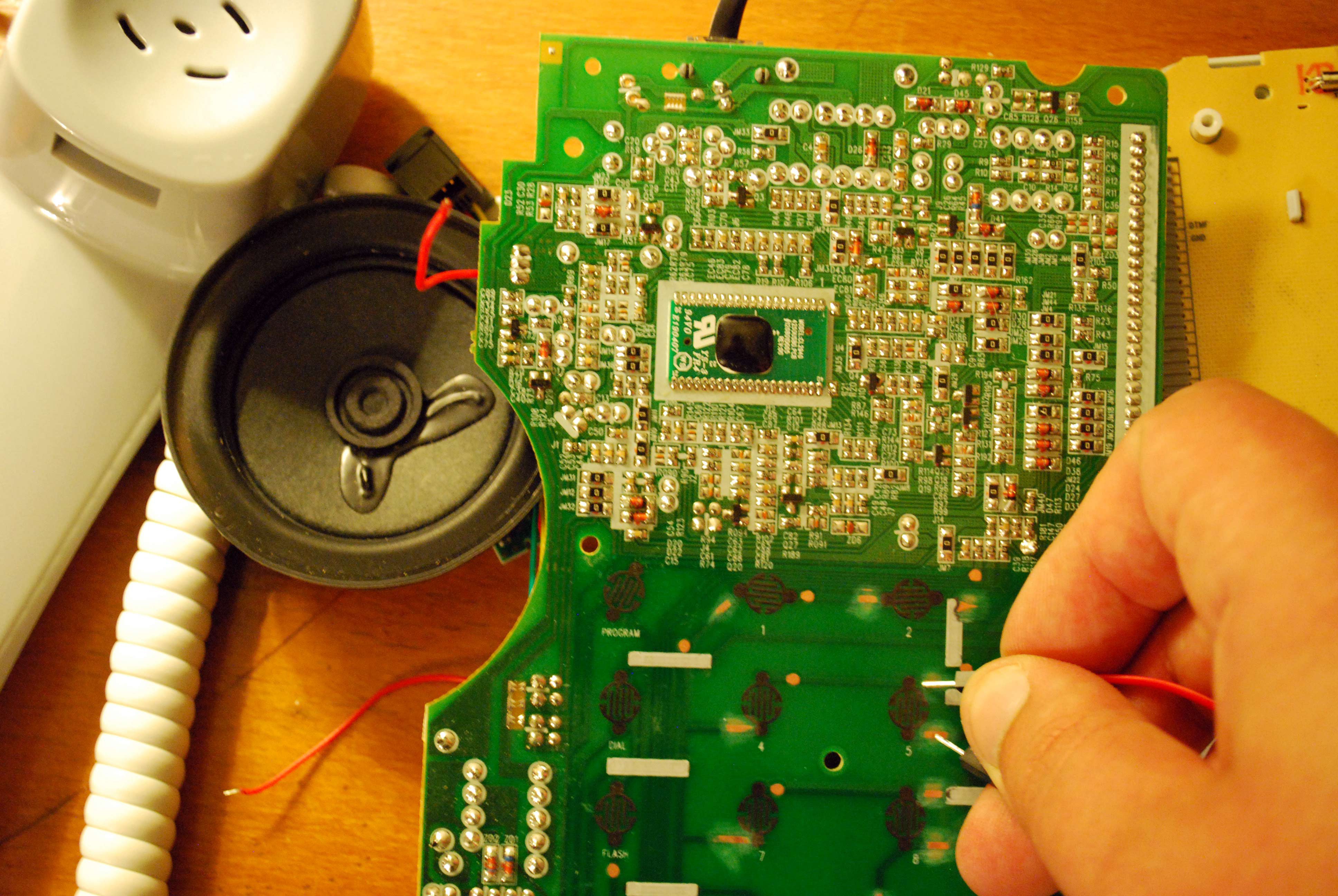
- For one, this phone's PCB makes it pretty 'easy', as all the button functions (i.e. numbers, etc) are listed clearly on the top silkscreen.
- The goal of at least this project, as mentioned, is to preserve the functionality of the original phone, so I chose points in the matrix 'outside' of the black carbon touch points, but not 'too' far away as to be unable to be jumpered with a DIP transistor.
- It does take a tiny bit of effort to take the mask of, but there is no need to press too hard. Just 40 seconds of gentle scrubbing not only reveals the underlying trace, quite cleanly, but also in contrast to other abrasive methods does not remove the copper.
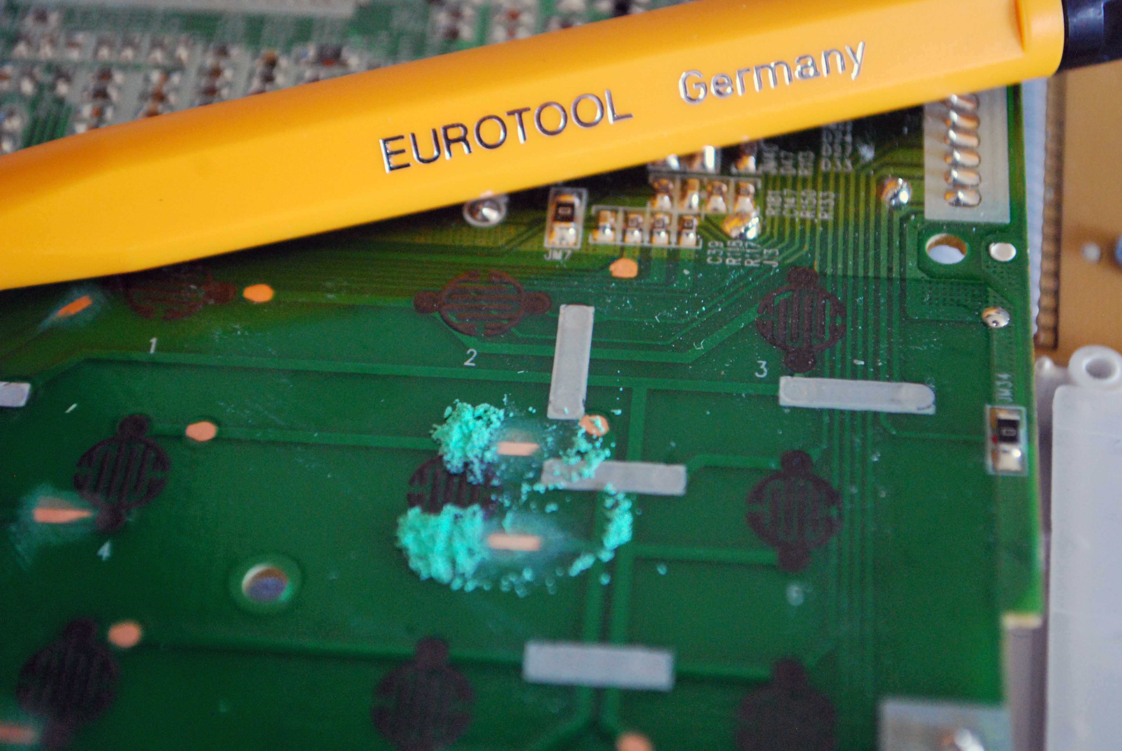
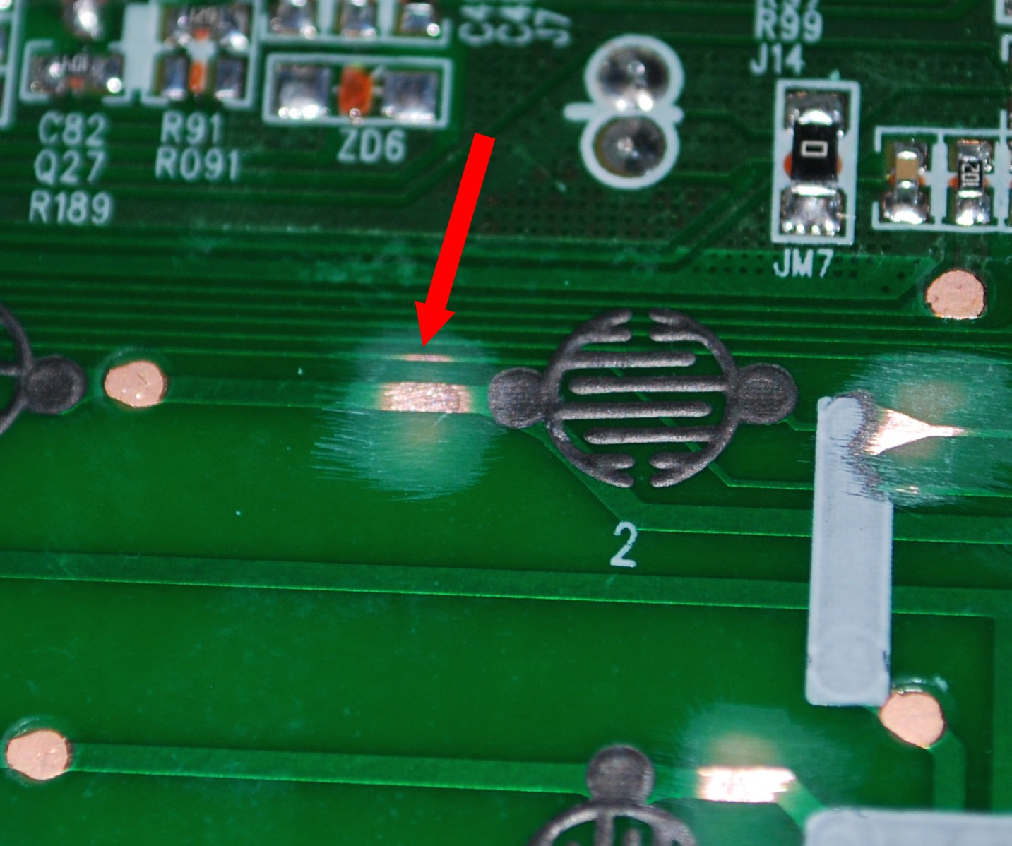
- As this was my first time using such a pencil for this purpose, I did make one mistake early on, I should have anticipated, but regardless here, also, is how to solve it. The pencil itself is of a reasonable width, which makes it great for the really 'wide' traces generally seen here. But a few of them on the board are either small, or in a tight corner beside other thin traces. If not careful you may expose other traces you did not mean to, which in of itself won't really 'effect' anything here, but will be a potential problem when we go to solder, as the solder mask is typically repellent. Easy way to solve this is just to use a piece of electrical tape to masque your circuit. A 'mistake', first seen below, and then the masque, in another use case:
![]()
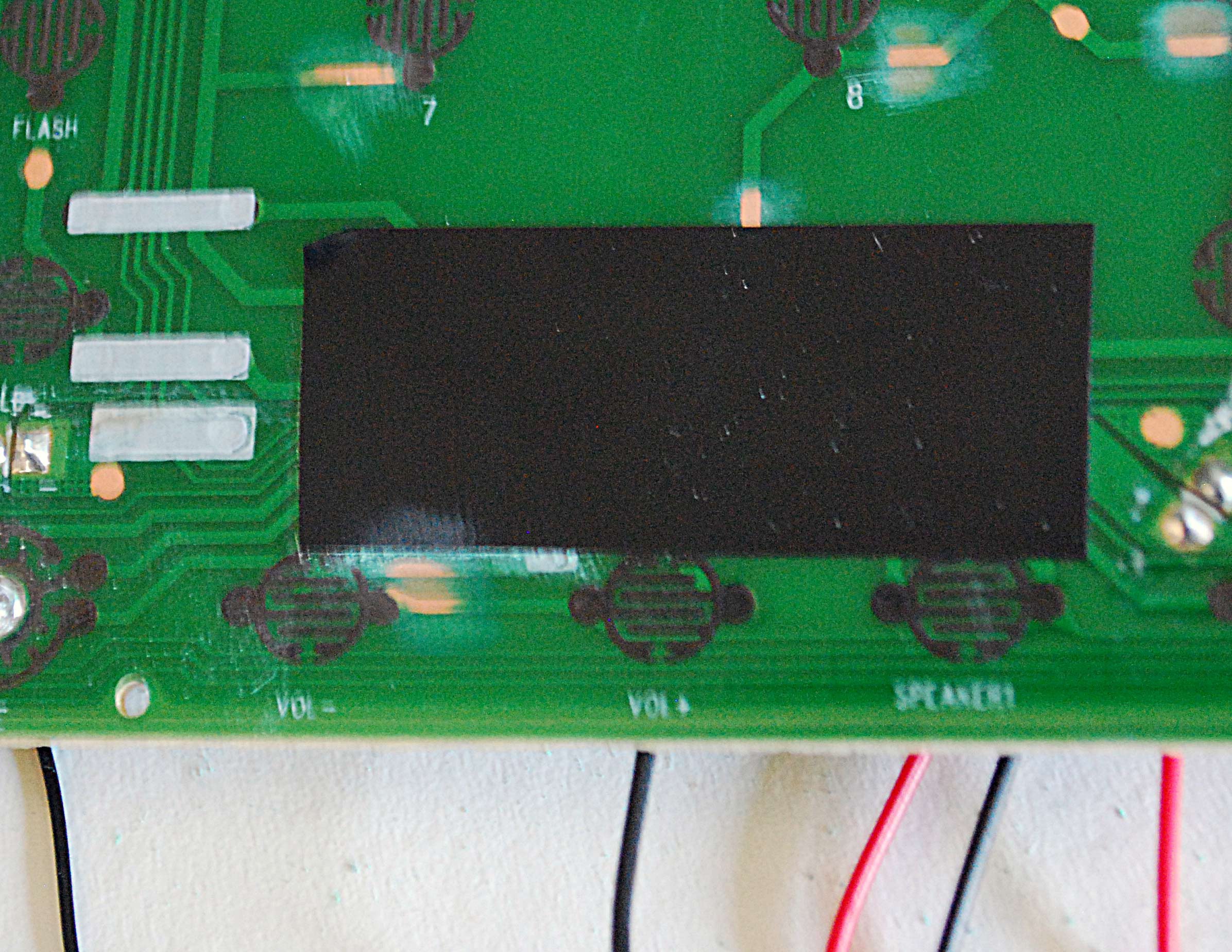
- And that is pretty much all there is to it... Only, a couple of additional things. I could have given access to 'all' the buttons, but at least at the present time for this project, they are just the numbers '0-9', the 'volume rockers' and the 'speaker'. '#/*, dial, memory, and other keys could be added in just the same way, but I don't immediately anticipate their use case here.
- Next, 'as is' we plug in the line and headset and with a spare wire jumper each of the connections just to ensure everything is 'kosher' (or one should hear the tone of a button, now 'virtually', or rather 'truly' being pressed, and it should be a different tone for each jumper point).
- I also made something of a 'rough sketch' along the various points and where I decided to pull out the traces:
One last thing is just to ensure we are using an 'appropriate' transistor for the application, also worth pulling out the multimeter and jumping a connection in just the same way so as to measure current flow.
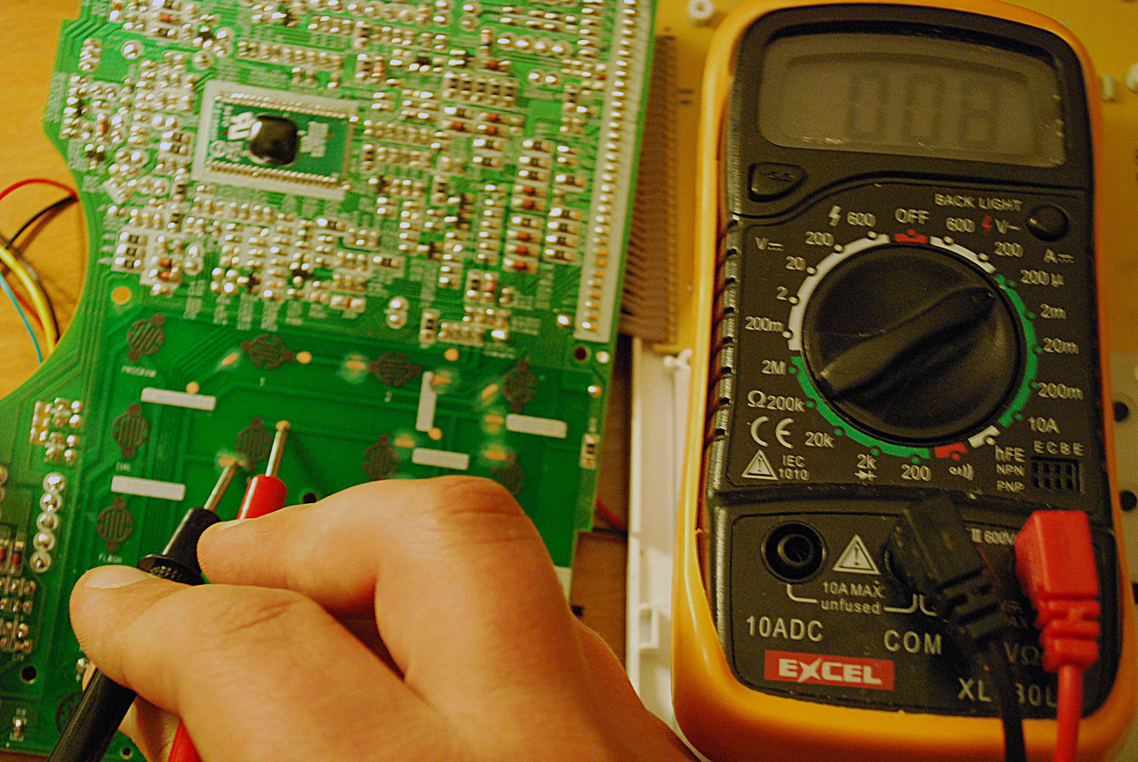
As I had expected in a modern circuit like this, current draw is really, really small on the order of .08 µA or 'microamps'.
Thus a selection of NPN Bipolar PN2222 transistors should be just fine.
Discussions
Become a Hackaday.io Member
Create an account to leave a comment. Already have an account? Log In.