 Howard Jones
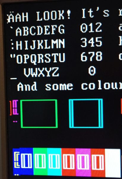
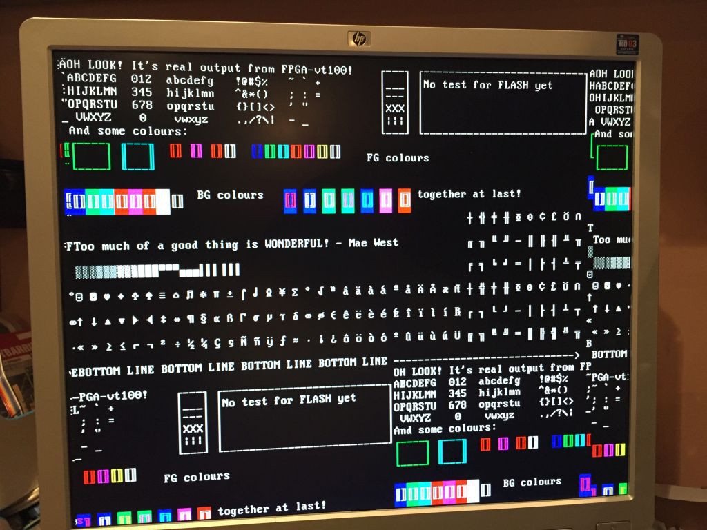
Inspiration material (although not directly useful): The original vt100 technical manual. I didn't know they could overlay video!
This uses quite a few tricks to get around slow memory, and bus contention between CPU and display controller, like a one-line buffer for the "in-hand" line, and a quick DMA to grab that line. It also describes the very low-level way that double-height and double-width mode worked (it halved the clock for a the line counter, or shifter, logically enough).
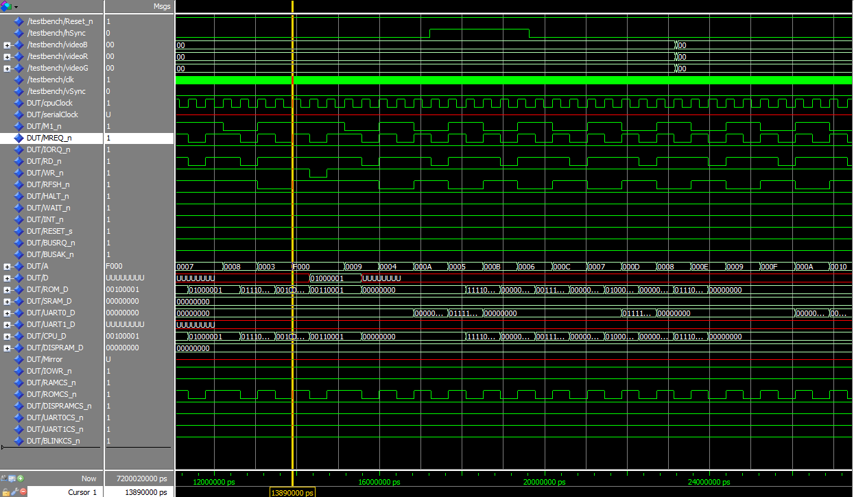
I think that I can get away with processing the buffered serial input in the vertical blank, like ZX81 Slow Mode would, and not worry about memory contention or similar.
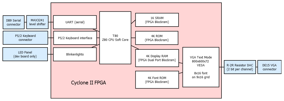
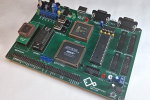
There's a github repo with my VHDL code in it (and eventually the Z80 assembly too): howardjones/fpga-vt. It's my first attempt at an HDL implementation (or any significant-sized digital logic actually, I'm a software person), so please be gentle.


 Colin Maykish
 Keith
Keith
 Hayden Kroepfl
 Maarten Janssen
Display memory contention was a problem back when memory was expensive. In many an FPGA today, it's easiest to have two screen buffers, one for random access from the CPU, another for display. Sometime during the vblank interval, the the random-access RAM gets copied to the on-screen RAM. This can be very fast - using a wider data path than the CPU uses, and a much shorter end-to-end delay. So while let's say the CPU core may need to run at CLK/2 or lower, the RAM copy can go full blast.