rolmie
-
Closeups
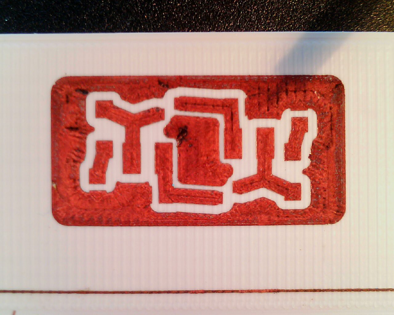
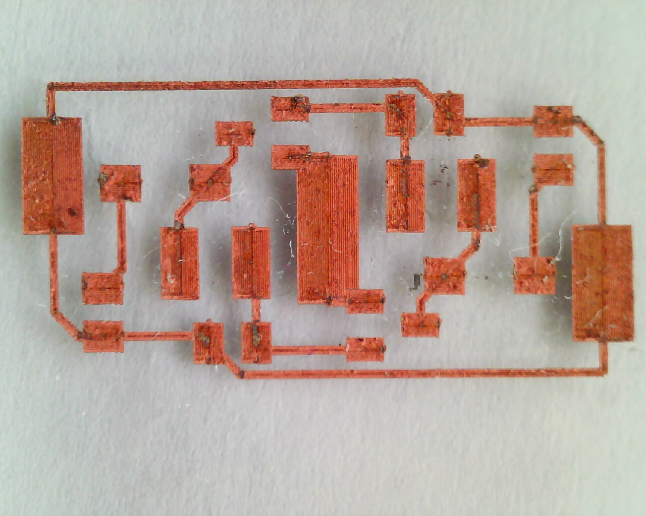
03/24/2018 at 20:46 • 0 commentsThe dimensions are about 2.5cm x 1.25cm (1"x0.5"). The features and footprints are well 'hidden' in somewhat oversized traces, but this is an easy way to reduce resistance.
Printing strategy is to print as many "shells" as possible, as I suspect that conductivity along the printed lines is better than across. Additionally each layer is cured twice, interleaving the lines. The laser spot is about 0.1mm in diameter, the feedrate is 33mm/s. Curing a single layer at this size takes about 4:30 minutes.
![]()
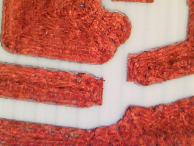
A well hidden SOT-23 footprint.
![]()
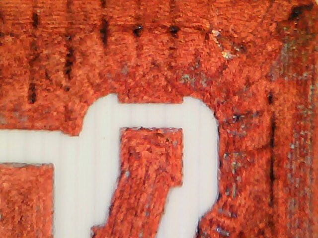
A 0805 foot print for a resistor:
![]()
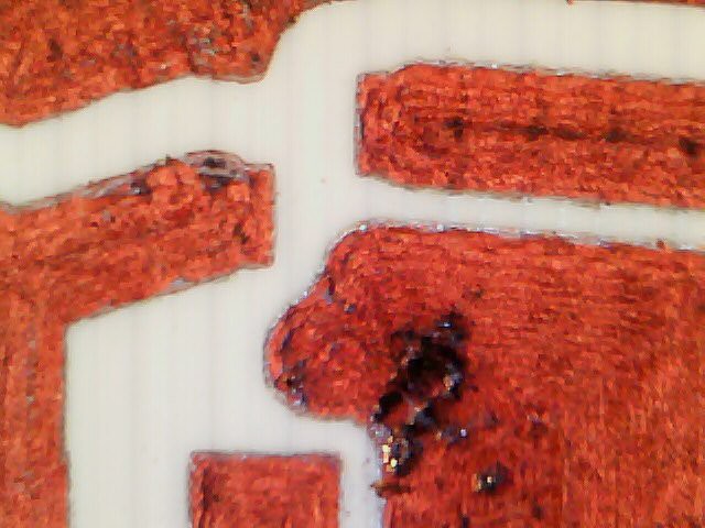
A "defect", reason unknown
![]()
-
Explaining the samples
03/24/2018 at 18:33 • 0 commentssubstrate: white PET-G
precursor: saturated Copper(II) formate solution, with about 5% (by weight) glycerol
process: window cleaner as wetting agent, 3 layers with 50% power increase per layerThe resistance measured from bottom-left corner to top-right is below 1 Ohm. The dimension of the sample are about 2.5cm x 1.25cm (1"x0.5").
![]()
substrate: glass (microscope slide)
precursor: saturated Copper(II) formate solution
process: dishwasher detergent as wetting agent, 2 layersGlass seems to be the easiest of all substrates, it is impossible to irradiate with too much power.
Tin bismuth solder (melts at 138°C) seems to work (limited experience). The footprints are SOT-23 and 0805 mostly, traces are about 10mil.![]()
substrate: polyimide (Kapton) on glass (microscope slide)
precursor: saturated Copper(II) formate solution
process: dishwasher detergent as wetting agent, single layer
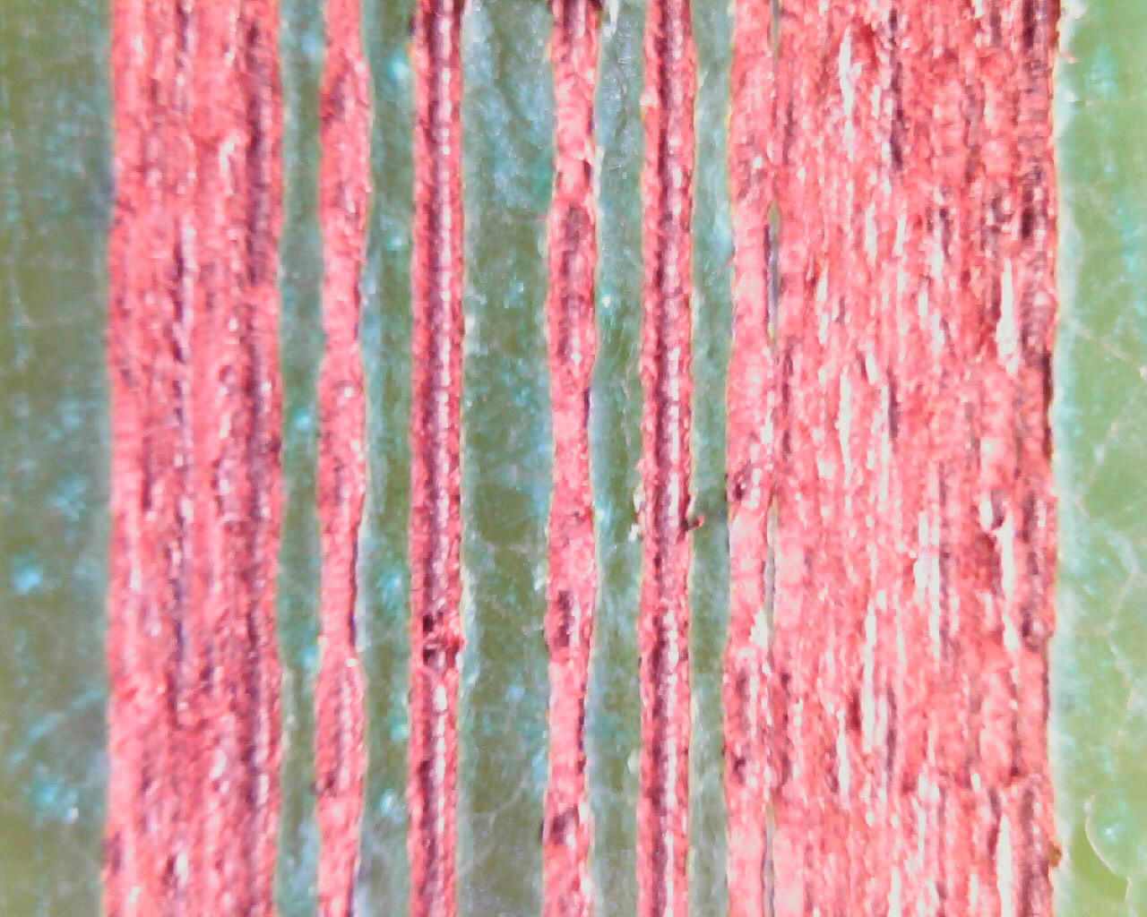
The distance between the traces in the center is about 0.5mm (20mil), based on that the trace width is estimated as 0.15mm (6mil). Lead Tin flux dissolves the copper.![]()
substrate: fiber reinforced epoxy (FR4)
precursor: saturated Copper(II) formate solution
process: dishwasher detergent as wetting agent, single layerTin Lead solder doesn't work.
![]()
PRINTED! circuit boards
Laser induced copper deposition from a liquid precursor on different substrates, including 3D printed parts.