 Sander van de Bor
The Arduino Core is ready! Find the core on:
https://github.com/SpenceKonde/megaTinyCore
Please report all issues.
Introduction
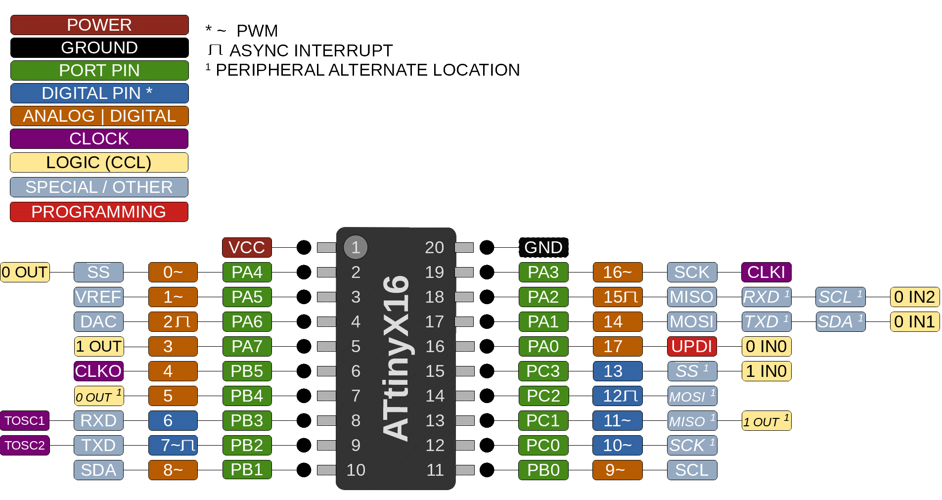
ATMEL was acquired by Microchip Technology in 2016 and last year they came out with a new microcontroller family sharing their technology, the tinyAVR and megaAVR. Out of this new offering the ATtiny1616 draw my attention. Looks like it has all the benefits from the ATtiny84a, same foot print, same power specifications, and some great additional features as well as you can see in the table below:
| MCU name: | ATtiny84a | ATmega328P | ATtiny1616 |
| Operating Voltage: | 1.8 - 5.5V | 1.8 - 5.5V | 1.8 - 5.5V |
| Digital I/O pins | 12 | 23 | 18 |
| PWM Digital | 2 | 6 | 6 |
| Analog Inputs | 8 | 6 | 12 |
| Analog Outputs | 0 | 0 | 1 |
| Flash Memory | 8 KB | 32 KB | 16 KB |
| SRAM | 512 | 2048 | 2048 |
| EEPROM | 512 | 1024 | 256 |
| Clock Speed | 8 MHZ | 20 MHz | 20 MHz |
| Size | 3x3 body | 4x4 body | 3x3 body |
| Timers | 1x8b, 1x16b | 2x8b, 1x16b | 1x12b, 3x16b |
| Digital Communication Peripherals | USI (~SPI) | UART, SPI(2), I2C | UART, SPI, I2C |
Able to run this from the 20 MHz internal oscillator, twice as much flash and four times more SRAM (compared to the ATtiny84) and support of most common peripherals excites me! There are just some minor problems. There is no Arduino support (yet) and there is no DIP version to plug into a breadboard.
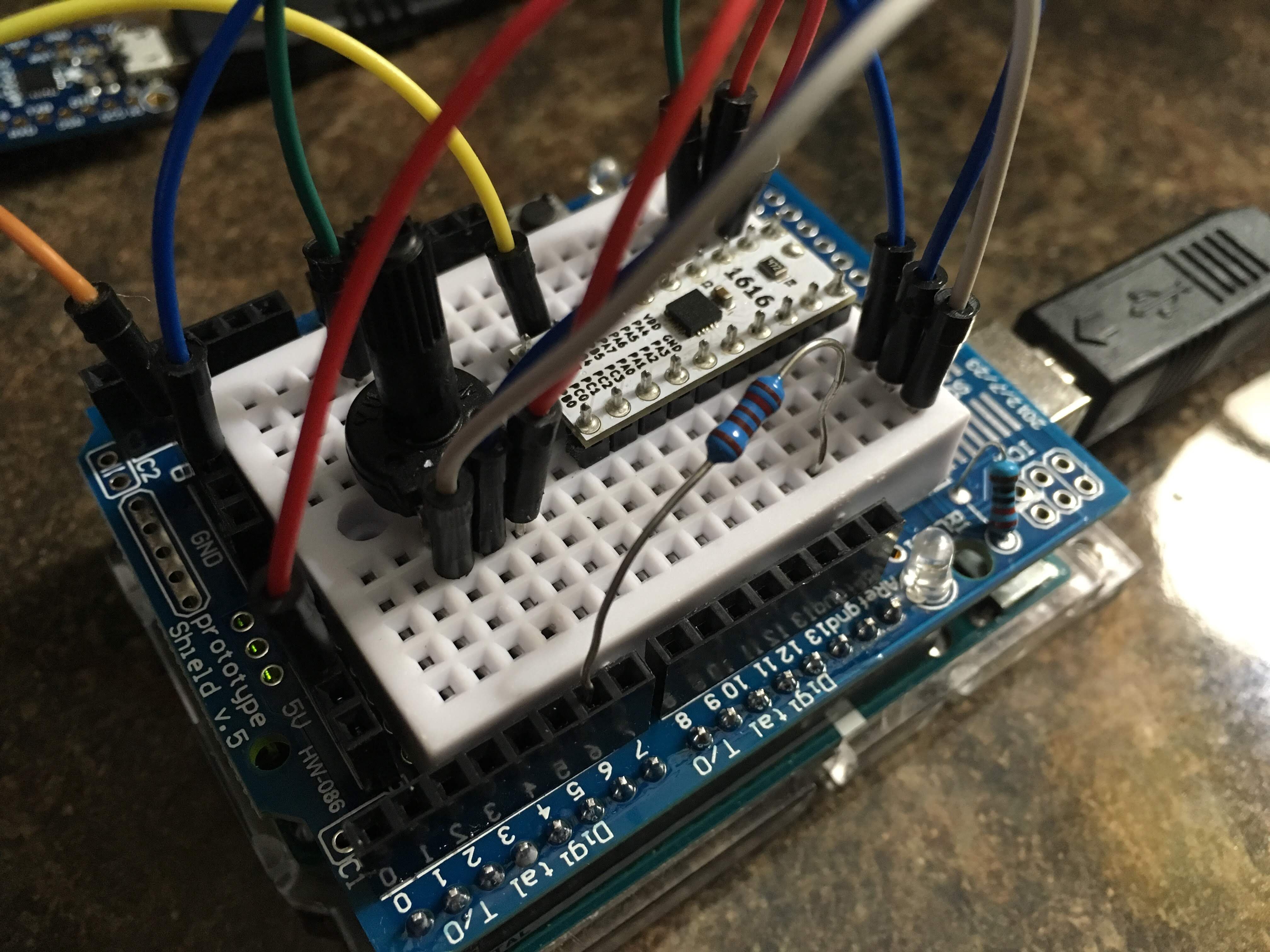
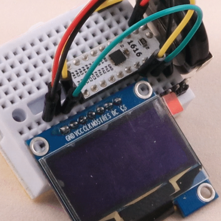
This project will document the development of the Arduino Core for the tinyAVR 1-series and a breakout board for the ATtiny1616. Throughout different logs different challenges will be explained and resolved.
A regular Arduino UNO can be used to program the ATtiny1616:


 Simon Merrett
 Sagar 001
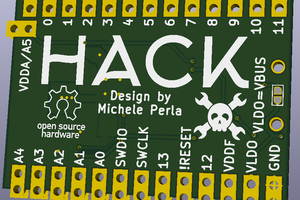
 Michele Perla
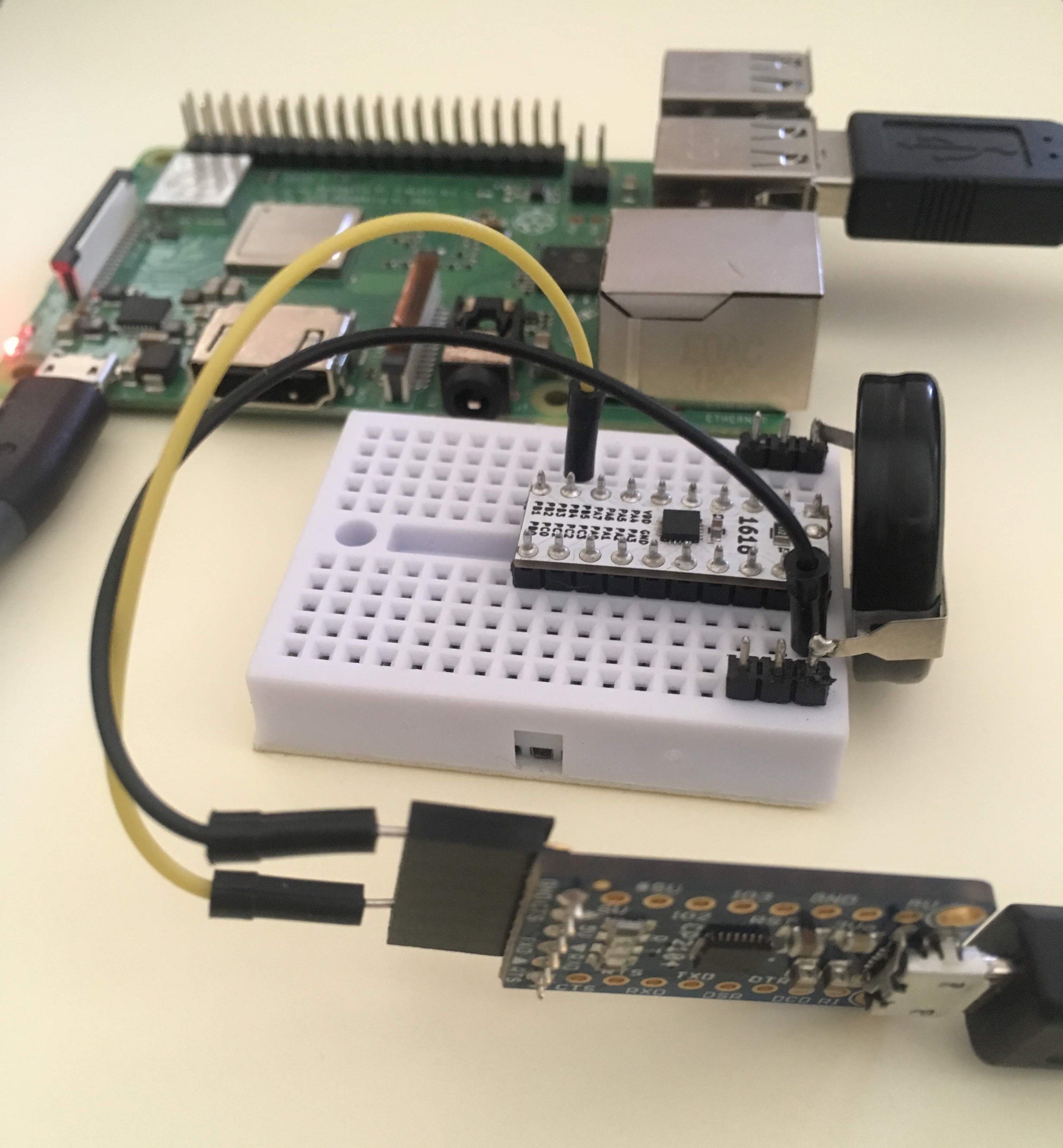
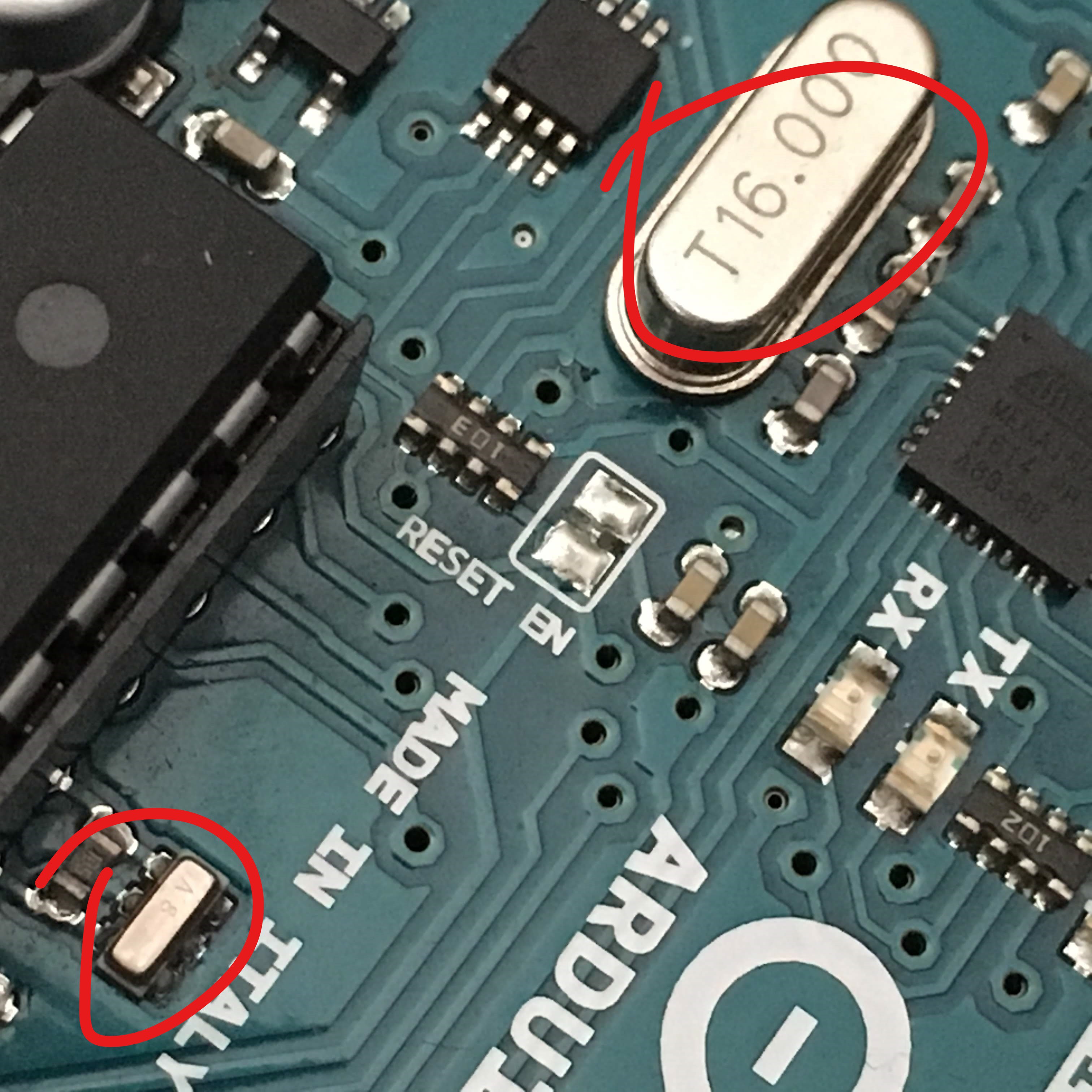
I've been using the 3217 extensively for the last few months, so much so that I gave Blue Board #01 the appropriate 24-pin VQFN footprint. I have also been using the 1616, 416 and 404. In my case, I've been using an Atmel ICE (left over from a previous project). I'm also planning to get hold of the $15 MPLAB Snap programmer.
With regards to the reset pin: the factory default configuration allows the reset pin to be used for programming without any further configuration.
Like Simon, I'm very much looking forward to hearing how you got the Arduino bootloader and environment going!