Close
0%
0%

10mbps over 1km on a single pair of wires

A simple 46mmx22.5mm module to route power and differential signals (RS-485) over RJ-45

Similar projects worth following
μDiff provides an easy way to reliably transfer power and a digital signal over a long-distance using an inexpensive RJ-45 cable. This can be useful for large robots, LEDs, or any device that needs reliable communication over more than a few meters.

It uses RS-485 differential signaling and 802.3af Power-over-Ethernet pinouts to achieve this. It can accept an input voltage between 6.5V-12V, and provides outputs of 5V and 3.3V. All signals and voltages can be accessed through a 10-pin header.

Current is limited to 1A. Beware of current limitations on the RJ-45 cable, it's typically ~350mA for an AWG26 shielded wire.

Most components are pre-soldered SMD (0603, 0805), while the rest are easy to source off-the-shelf through-hole pin headers and RJ45 connectors.

The board measures 46mm x 22.5mm, lead-free and RoHS compliant, and is stackable through 4xM2 holes (one hole is tied to GND).

How it works

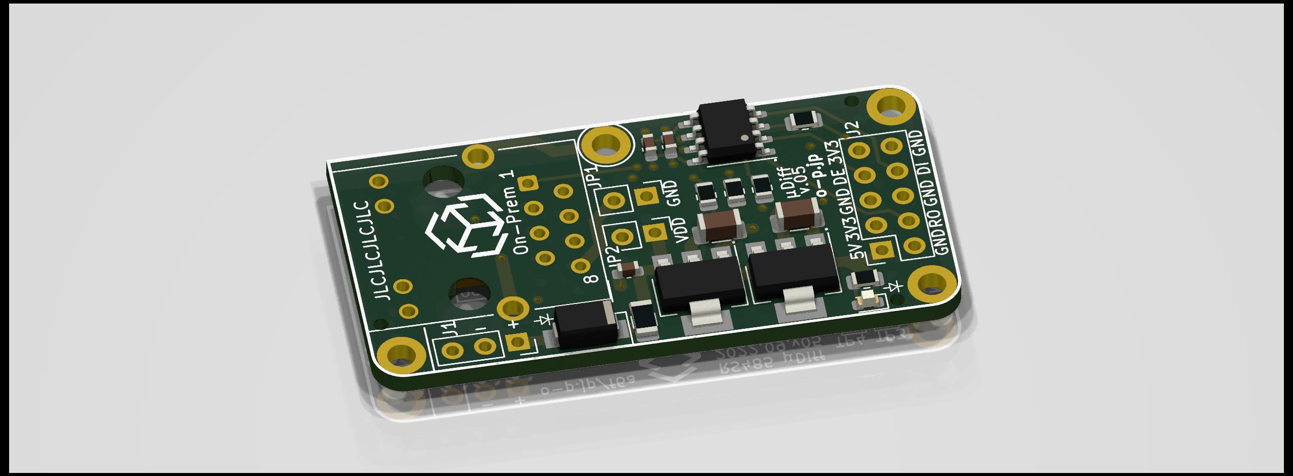
At first glance it should be obvious how this module works, but I'll explain it below.

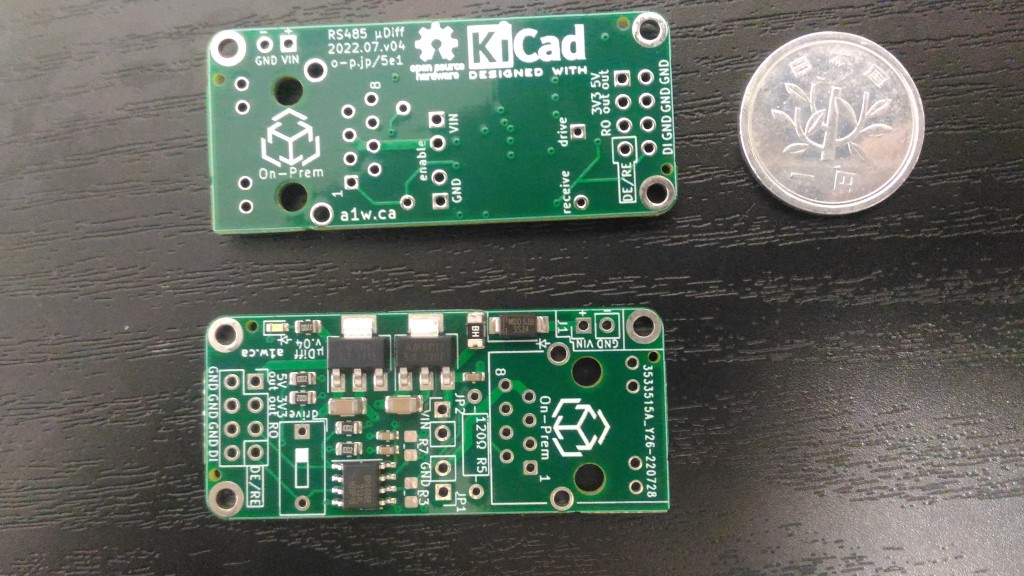
To start, you need minimum 2 modules.

Let's assume one device acts as the driver, and will be connected to an MCU (microcontroller, ex: Arduino).

The other device will act as the receiver, and will be a short string of WS2812 LEDs drawing 200mA of current at 5V (1W).
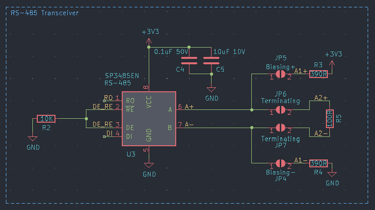
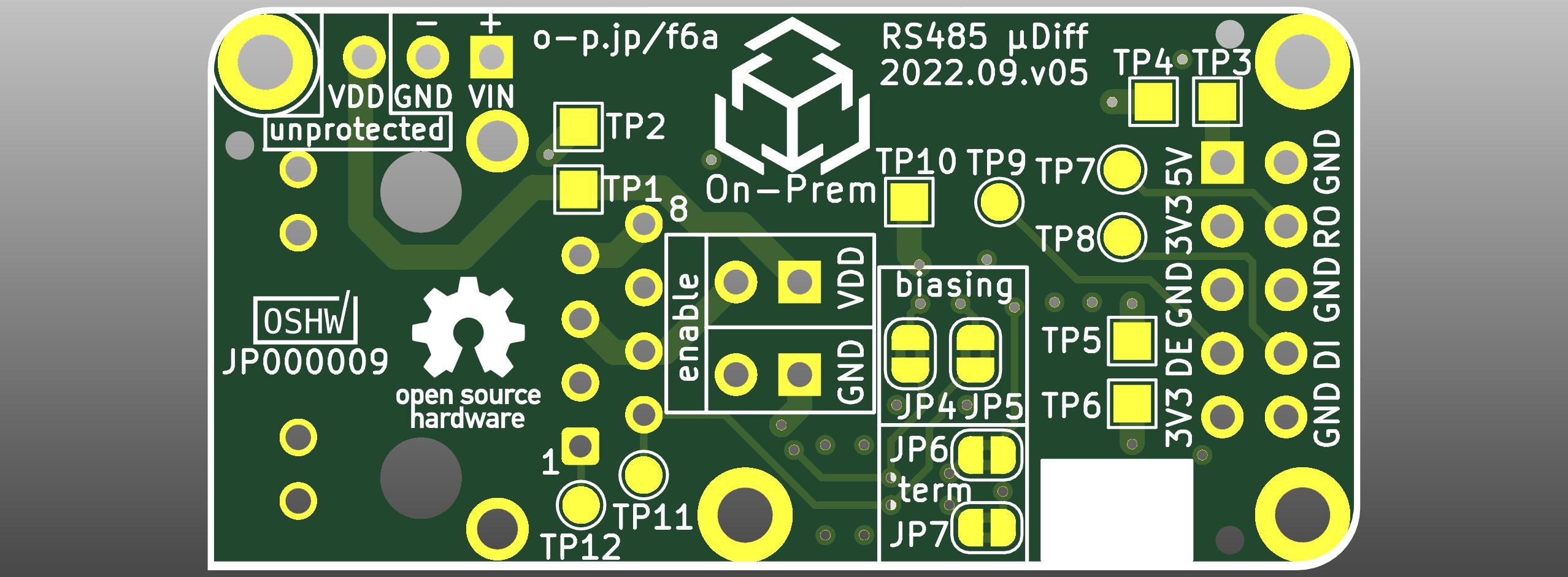
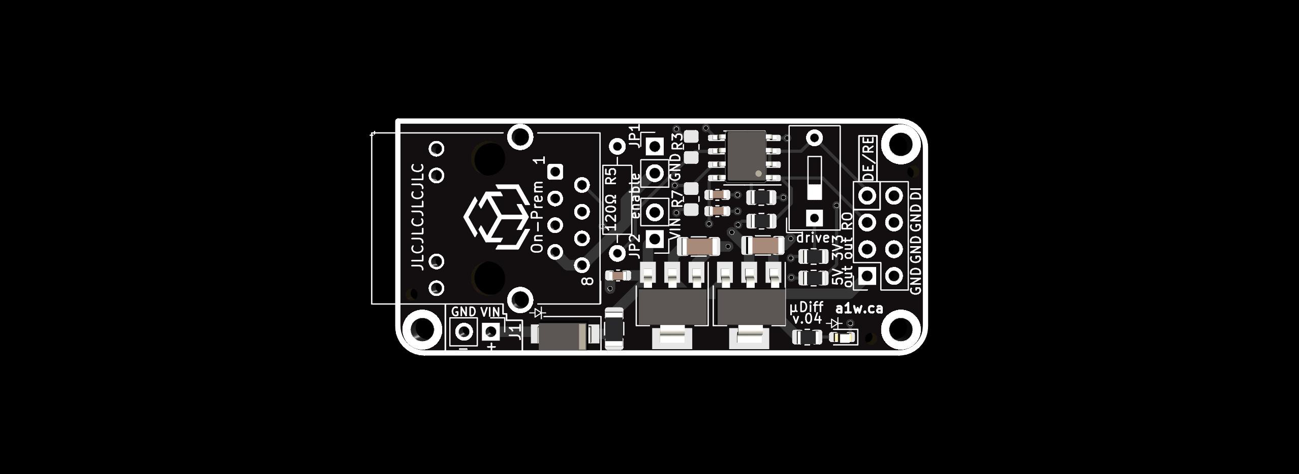
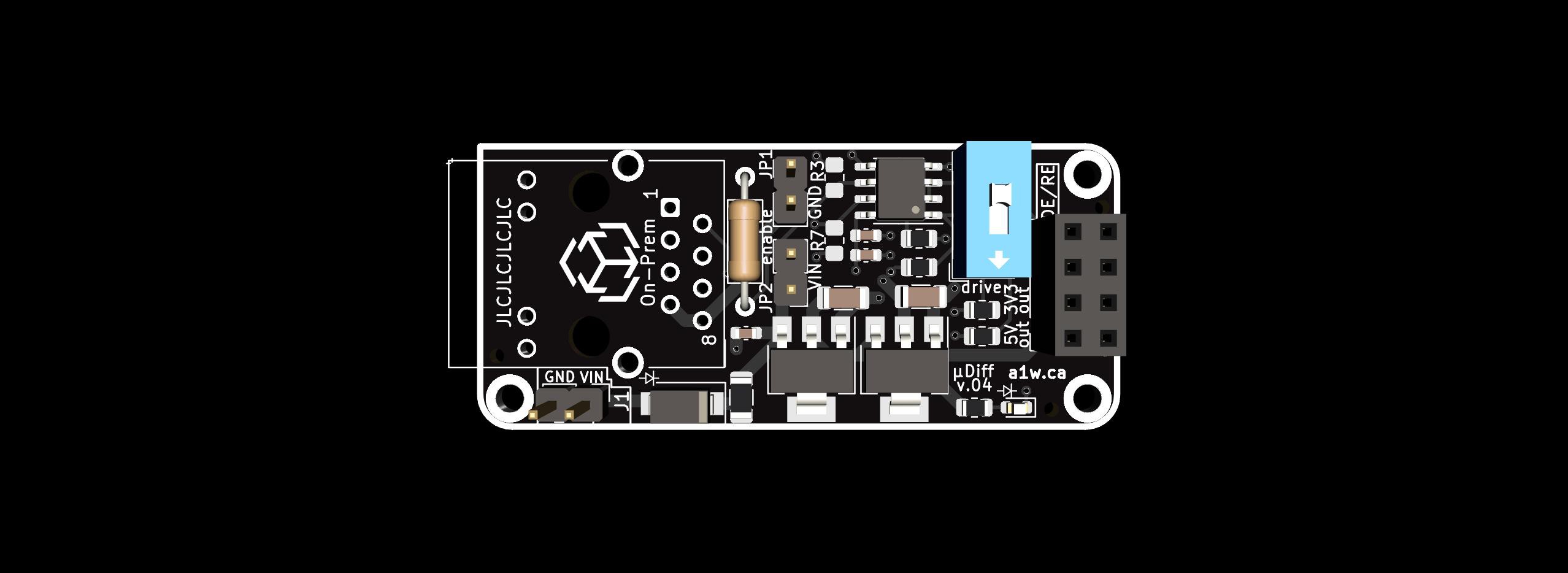
Connections

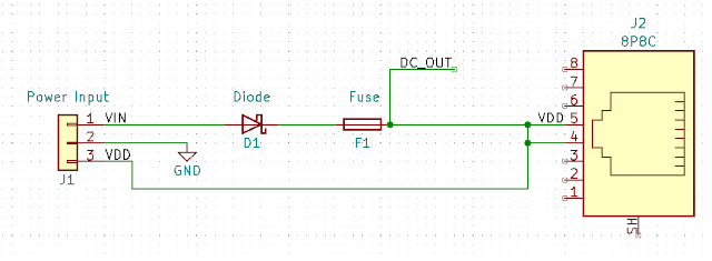
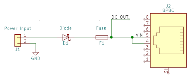
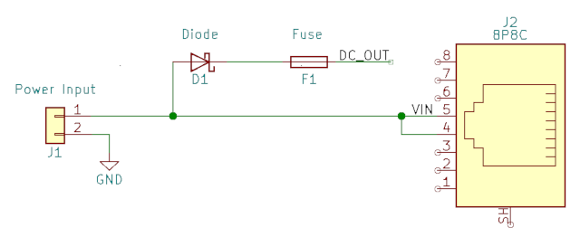
The two modules will be connected through a 15 meter AWG26 RJ45 cable, and we'll assume there's a 12V power source near module 1.

  • Connect the 12V and GND from your power source to the VIN/GND pins on module 1
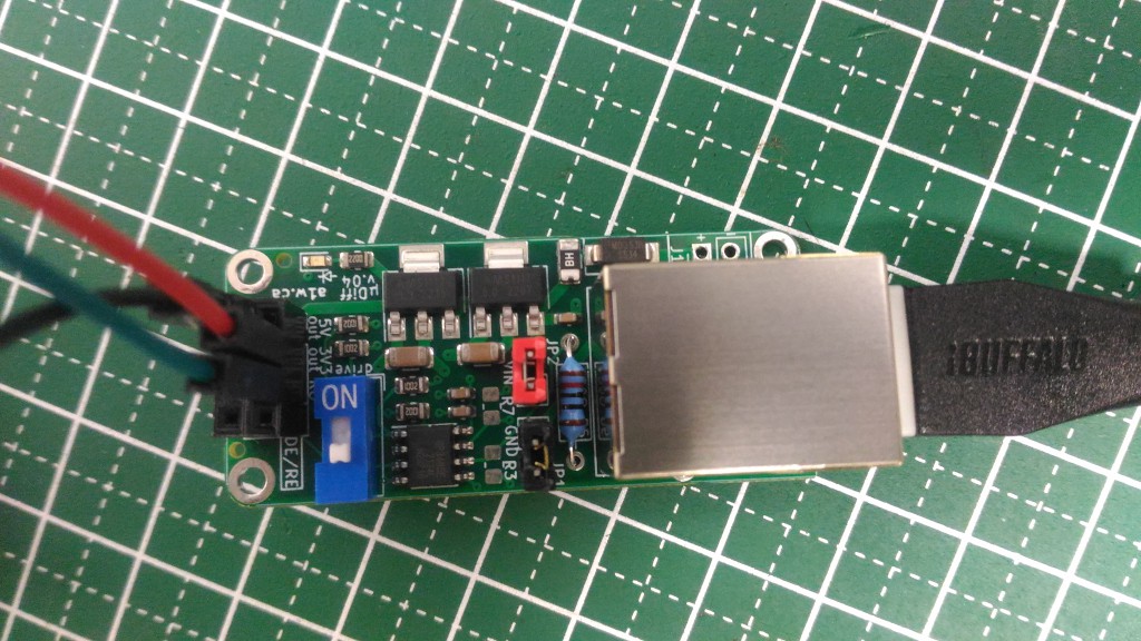
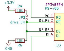
  • Connect the 8-pin JST cable to module 1 and wire the other end to the MCU's data pins (and power/gnd if needed), and ensure RE and DE are pulled high (DIP switches in the OFF setting)
  • Connect the RJ45 cable between the two modules
  • Connect the 8-pin JST cable to module 2 and wire the LED strip to it, and ensure RE and DE is pulled low (DIP switches in the ON setting).
  • Profit!
                                                  +-----------------------+
                                                  |         Device        |
                                                  |    (5V LEDs WS2812)   |
       +--------------+                           |                       |
       |   +6.5V~12V    |                           |    +---------------+  |
       | power source |                           | DI |          VIN GND |
       +-+----------+-+                           +-+--------------+---+--+
         |          |                               |  |           |   |
+--------+----------+--------+                   +--+--+-----------+---+------+
|  (+) VIN          GND (-)  |                   | RO RE DE DI GND 5V GND 3V3 |
|                            |    15m AWG26      |                            |
|       RS485/RJ45     +-----+ <-+-+-+-+-+-+-+-> +----+  RS485/RJ45           |
|         module 1     |RJ45||   | | | | | | |   |RJ45|    module 2           |
|         (driver)     +-----+ <-+-+-+-+-+-+-+-> +----+   (receiver)          |
|                            |                   |                            |
| 3V3 GND 5V GND DI DE RE RO |                   |  (-) GND          VIN (+)  |
+------+---+-----+-----------+                   +----------------------------+
       |   |     |
    +--+---+-----+---+
    | GND VIN   P0   |
    |                |
    |       MCU      |
    |    (Arduino)   |
    +----------------+

Of course you'll also need to push some code to your MCU to drive the DI data pin and transmit the signal to the LEDs.

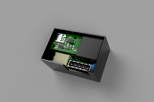
This project is certified open hardware:


Similar projects

  • 1 × RJ45 connector
  • 1 × 10-pin 2.5mm female header (2x5P)
  • 1 × 3-pin 2.54mm female header (1x3P) with jumper
  • 2 × 2-pin 2.54mm male header (1x2P)

  • Publlished the latest KiCad files to GitHub

    Alexander Williams01/24/2023 at 03:10 0 comments

    I've finally uploaded the latest v.05 KiCad files to GitHub. I've decided I won't be selling these boards because I don't want to deal with the logistics of it, and I just don't care enough haha.

    Everything is open source so you're free to download the files and have the boards built yourself by a nearby manufacturer.

    Stay tuned for my next projects, which I believe will be slightly more interesting and useful.

  • Received the v.05 PCBs, and they're almost perfect!

    Alexander Williams10/16/2022 at 08:59 0 comments

    I received the v.05 PCBs a couple weeks ago and performed the usual series of tests and burn-in. So far I am extremely satisfied with the way they work - perfectly - but I'm concerned about a some heat dissipation and potentially high current draw.

    I'm not yet sure if it's caused by the blue LED which I fitted onto the board, or the low-value biasing resistors...

    I'll perform some more tests this coming week and then publish my results, pictures, etc.

    I'm aiming to place them online for sale on Tindie within the next 2 weeks, so stay tuned for that.

  • Ordered the v.05 PCBs

    Alexander Williams09/12/2022 at 07:36 0 comments

    I finally ordered the v.05 PCBs after making one final change:

    Rather than connecting the 8P8C connector shield pins to GND, I tied them to "Earth" which is tied to the M2 mounting hole (H2) right behind the 8P8C connector. I also added another solder bridge jumper (JP3) which would allow you to tie "Earth" and GND together.

    The idea is the PCB, when mounted in an enclosure, can be tied directly to real "Earth" through one of the mounting holes. Wiring the 8P8C shield to that is also a good idea, to reduce EMI radiating from the RJ45 cable. In many cases it would be important to also tie the PCB ground (GND) to "Earth", but I wanted to leave that optional, so I added the solder bridge jumper (JP3).

    I should receive these boards in ~2-3 weeks depending on the weather (it's typhoon season here in East Asia). As usual, once I receive them i'll run some tests and confirm everything before making them available on Tindie.

    Stay tuned!

  • RS485 schematic breakdown: optional resistors

    Alexander Williams09/07/2022 at 05:51 0 comments

    As mentioned in my previous post, I've changed the way the resistors are wired in v.05 of this module. Below I'll breakdown the RS485 schematic sub-section and explain how I did things this time around.

    From left to right, I used a 10K pull-down resistor (R2) on the DE/RE pins, which are tied together for simplicity. This value is strong enough to bring the pins LOW, yet weak enough to bring them HIGH if you time them to 3.3V (can be controlled by an MCU pin).

    The RS485 IC (U3), a MaxLinear SP3485EN SOIC-8 pin chip is featured in the middle. You can also see two ceramic non-polarized decoupling capacitors (C4, C5) routed to 3.3V and GND. The capacitor voltages have been derated by more than 50%.

    Next we have the A and B pins for the RS485 differential signal. I labeled the nets A+ and A-, as this allows me to route differential traces to the RJ45 (8P8C) connector pins 2 and 1. The RJ45 connector pin 2 is routed to the A+ net, and pin 1 is routed to the A- net.

    For fail-safe biasing, there is a solder jumper (JP5, JP4) routed to the pins 6 and 7 respectively on the RS485 IC (U3). Pin 2 on the jumpers are wired to 390Ω resistors (R3, R4). I also labeled the nets A1+ and A1- to make things easier in KiCad's PCB Editor.

    Finally, for terminating, there is also a solder jumper (JP6, JP7) routed to the pins 6 and 7 respectively on the RS485 IC (U3). Pin 2 on the jumpers are wired to the same 100Ω terminating resistor (R5). With this size resistor and the IC running at 3.3V, it should be sufficient to create a differential voltage greater than 200mV.

    The solder jumpers are pads on the bottom (back) of the PCB. Each jumper has 2 pads separated by a little space. A small blob of solder can be used to join the two pads and create a connection, thus closing the circuit and enabling the resistors. It's important to join both biasing solder jumpers, or none at all. It's also important to join both terminating solder jumpers, or none at all.

    For a typical use-case, you would join all four (4) solder jumpers on the first end node (JP4, JP5, JP6, JP7). Then, you would only join the terminating solder jumpers (JP6, JP7) on the other end node. Every other node in between would not need any solder jumpers connected - since the bus will be properly terminated and biased.

    The reason solder jumpers are used is because they require very little board space, and they're easy to solder together (compared to soldering tiny resistors). Also, once the jumpers are enabled, you typically don't need to change or disable them. This was a much better alternative to using a 4-position DIP switch or 2.54mm through-hole jumper headers. The cost of the resistors is so low that it made sense to simply populate every board with them, even if they won't be used.

    Next, I will attempt a SPICE simulation before ordering the prototype batch of v.05 PCBs.

    Stay tuned!

  • Resistors for RS485 ICs: not necessary?

    Alexander Williams09/02/2022 at 07:00 0 comments

    Resistors in El Cheapo

    While running more tests on the v.04 module, I discovered another issue which wasn't immediately obvious.

    On the internets, the below schematic is quite popular:

    It's a schematic for the ultra-low-end RS485 module using the MAX485 IC, you can find it on Amazon/eBay/AliExpress for like $2 or something.. remember "El Cheapo":

    Well, there's more to that story.

    Copying garbage

    When I first created this project, I copied that schematic's design and integrated it to my module. That was a big mistake because it had some bad engineering implemented on top of the bad physical shape:

    • Every data line is pulled high with a 10K resistor - even the outputs. This means the module itself is set as a "driver" by default, and you know what happens when you connect two RS485 drivers together? bad things.
    • There is a 120 ohm terminating resistor on the A+ & B- lines. This means your bus is limited to only TWO (2) of these modules unless you desolder that resistor from the other modules.
    • There are 20K fail-safe biasing resistors on the A+ & B- lines. This means the voltage drop will be too large (because there's also terminating resistors) and the 20K resistors will be useless - in fact, they won't even do their job of bringing the differential voltage between A&B higher than 200mV when there is no driver on the line...
    • ... However, because the receiver output (RO) pin is already tied HIGH by default (10K resistor), the above point is moot.

    Isn't that ironic? The board is poorly designed yet it magically works thanks to that poor design. Even more hilarious is that I copied it in my v.03 modules and it also worked perfectly!

    Confused? Here's more details

    Older RS485 ICs had very basic "fail-safe" feature where the RO pin would go HIGH when the input pin is left floating or shorted. The RS485 IC's fail-safe feature took care to place that pin HIGH when the voltage difference between the A+ & B- lines are greater than 200mV (that's how it detects "high" or "low" on the A+ & B- lines). Unfortunately that assumes there are no terminating resistors between A+ & B-. For that reason, people used to place "biasing resistors" on the A+ & B- lines. The resistors would be identical, A would tie the resistor to +5V (the MAX485 runs at 5V) and B would tie it to GND. Doing so creates a voltage divider which - depending on the size of the resistors - can keep the voltage difference between A+ & B- above 200mV.

    (source: MaxLinear AN291 PDF) 

    Anything between 200mV and -200mV falls in the "indeterminate" zone: no-man's land for data signals, where the receiver is uncertain if it's seeing a 1 or a 0.

    When you use terminating resistors on the RS485 bus (one at each end - max 2), assuming 100 ohm terminating resistors between the A+ & B- lines, and RJ45 (cat5e?) wiring, the voltage will drop significantly.  Remember, it should be +/- 200mV, however with the above El Cheapo, basic math shows it would be between 0mV and 15mV. Oops!

    But El Cheapo works, everyone uses it!

    Actually no it doesn't work. The only reason "it works" is because to make it work, we always tie the pins to an MCU, and we always ensure the proper pin (input/output) direction, and we always use twisted wires between A & B, and we always ensure to only have ONE (1) driver on the bus, and we always only ever use 2 modules on a bus.

    So in an ideal wiring situation, all is well. However it will go to hell if you try to use more than 2 modules, or if you decide to set both modules to receive (pull RE and DE down to GND). The voltage difference between A+ & B- in that case will fall too low, moreover the 10K pullups on the data pins will contribute to overloading the bus - which is somewhere between not good, and bad... now, tell me "it works". Hah!

    Solutions

    For the eagle-eyed, you may have noticed I wrote "Older RS485 ICs". Newer versions of these ICs such as MAX3088 used in the v.03 module, have a differential voltage threshold between...

    Read more »

  • v.05 Sneak preview (updated)

    Alexander Williams08/28/2022 at 13:45 0 comments

    UPDATE: September 06, 2022

    In a previous post I said I won't make many changes to v.04, but it turns out there were more than a few things I didn't like about it.

    In v.05, I've made the following improvements:

    • Changed dimensions slightly, to 46mm x 22.5mm to accommodate the changes below.
    • Re-added a 4th mounting hole, because the PCB won't stand on 3 legs haha.
    • Replaced the through-hole "optional" terminating resistor (120Ω) with an 0805 SMD 100Ω resistor to match the characteristic impedance of a CAT5e or CAT6 cable. In a multi-drop configuration, the resistor can be enabled by soldering two bridge jumpers on the bottom of the board: JP6 and JP7.
    • Added 2 x 0805 SMD 390Ω fail-safe biasing resistors which can be enabled by soldering two bridge jumpers on the bottom of the board: JP4 and JP5.
    • Added a 3rd input pin for VDD on the header J1, which will bypass the diode and fuse and go directly to the 5V DC-DC converter and the RJ45 connector (if the VDD jumper JP2 is enabled).
    • Changed the orientation of the VDD/GND 2-pin jumpers JP1 and JP2.
    • Added test pads under the PCB for every signal and power rail.
    • Updated silkscreens on the top and bottom of the PCB.
    • Replaced 2x4 pin (8P) socket header with 2x5 pin (10P) and added an extra 3.3V and GND pair.
    • Removed the 10K pullup resistor on DE/RE.
    • Removed the DIP switch to enable "drive" mode. Simply tie DE to 3V3 with a jumper wire to enable "drive". Defaults to "receive" mode.

    Here's a preview of the bottom of the PCB, and the new testpads and solder bridge jumpers for enable biasing/terminating:

    As a side note, for those who don't follow my GitHub account, I've already published the schematic and PCB files for v.04, but I haven't updated the documentation since I don't plan on selling v.04. The updated documentation (for v.05) will be published once I confirm it's working as expected.

    Stay tuned!

  • It was a feature, not a bug

    Alexander Williams08/26/2022 at 08:36 0 comments

    In the previous post about the safety feature/improvement in v.04, I wrote that to improve safety, I don't connect VIN directly to the RJ45 connector without going through a fuse/diode first. This is good, but it's problematic.

    In the v.03 module, since the two were connected, it was possible to stack two modules and directly link the VIN from one module to the other. This was very useful for sharing a high voltage arriving through the RJ45 cable. So, as much as it may have been a safety "bug", it also served as a useful "feature".

    While creating v.05, I aimed to fix this by also routing the VDD line (unprotected VIN from the RJ45) directly to a pin header. It adds a bit of danger, but the safety feature of the VIN/GND pair is still there. This will be useful for stacking modules and daisy-chaining the power to multiple modules from a single input.

    As you can see from the image above, the current arriving from the RJ45 connector is routed to an additional pin. It's a simple (and dangerous) way to bypass the diode/fuse protection circuit. When stacking modules, one would simply need to connect the VDD pin (J1-P3) of one module, to the VIN pin (J1-P1) of the other module, and connect the GND pins (J1-P2).

  • Received the v.04 PCBs, but there's a fail

    Alexander Williams08/11/2022 at 16:28 0 comments

    I received the v.04 PCBs, but I unfortunately discovered a design error which causes a strange problem.

    After soldering a pair of PCBs and running some tests, I noticed the RS485 IC would not send a differential signal after power-on the device from a cold start (ex: 12V power adapter is initially unplugged).

    I first thought it was an issue with the power-on sequence due to the 5V and 3.3V DC-DC converters, but checking those voltages and ramp-up with the oscilloscope showed there's no issue. Also, the blue LED on both boards light up perfectly, which means sufficient power is sent at power on (at least 6.5V).


    I then monitored the different signals individually, and noticed the DE (driver enable) line was not being driven high after that power-on sequence. It was hovering around 1.28V, although it needs at least 2V to be considered high.

    A quick look at the schematic shows the culprit: a voltage divider! *facepalm*

    I tied DE and RE together to GND with a 10K pull-down resistor. I also added a DIP switch (JP3) to connect DE/RE to 3.3V through a 10K pull-up resistor. This creates a voltage drop that's too large for the IC to see a high on DE. I guess I'll fix that by replacing the 10K pull-up with a 4.7K.

    In the meantime, the temporary fix (if using the board as a Driver) is to add a jumper wire between the DE/RE and 3V3 pins on the 2x4P (8P) 2.54mm connector. It's also possible to drive DE/RE high using an MCU if there's an available GPIO pin.

    Since I'm back in KiCad, I'll use that opportunity to add some much needed test pads under the PCB.

    Otherwise, I'm pretty happy with the way the PCBs turned out, and don't plan on making other changes in the near future.

    More details in a future post.

  • Important safety feature in v.04

    Alexander Williams07/28/2022 at 13:50 0 comments

    If you look carefully at the v.03 schematic, there's a silly mistake I introduced which could be disastrous if the end-user is not careful with their wiring and setup.

    Let's first illustrate the Input current flow on the new v.04 module:

    Unprotected Power -> Diode -> Fuse <-> RJ45 / DC-DC Converter

    As you can see, the unprotected power, perhaps from a power adapter or bench supply, will first pass through a few components before going out the RJ45 cable, thus protecting it from shorts and overcurrent scenarios. The diode should also protect the power sources, should there be a power source at both ends.

    Now let's look at the Input current flow on the old v.03 module:

    RJ45 <-> Unprotected Power -> Diode -> Fuse -> DC-DC Converter

    Do you see the difference?

    What this means is, in the old v.03 module, unprotected power will flow directly through the RJ45 cable to the other module, without any fuses to protect the cable. Any short or overcurrent will flow freely through the cable and likely heat, melt, and burn it down.

    I noticed this problem when I first designed v.03, but it was already being produced and I could only hope to correct it in v.04 - which I did.

    Hopefully nobody made the mistake of 1) drawing too much current through the RJ45 cable, 2) powering both modules at the same time with the VIN enabled jumper set, 3) creating a short / over-current situation.

    As usual, since this is an open source project, I take no responsibility for any problems that may occur with your use of this PCB or design files. Create and use at your own risk.

  • v.04 Sneak preview: 1/2 width PCB

    Alexander Williams07/08/2022 at 14:22 0 comments

    Here's a sneak preview of v.04:

    It has some important changes which I'll list below:

    • The PCB is now exactly HALF the width of the v.03, at 50x22mm (instead of 50x44mm).
    • It's a 4-layer stackup instead of 2-layers, with 3.3V power and ground planes in the middle.
    • Through-hole 5V DC-DC converter is now SMD but has a max 12V/1A (15V absolute max)
    • Through-hole RS485 IC is now SMD and runs at 3.3V instead of 5V.
    • Through-hole fuse is now SMD 24V/1A (trip 1.8A).
    • GND and VIN are now simple pin headers instead of a large terminal block, since current is limited to 1A anyways.
    • DE and RE pins are tied together (to GND with 10K resistor, i.e: receive mode), but can be set to drive mode (to 3.3V) through a DIP switch. This means it's not possible to disable the RS485 IC anymore.
    • 8-pin JST output header is now a 2x4-pin female socket header, and since DE/RE are tied, there is now a third GND pin on the header.
    • Jumpers JP1 and JP2 can enable sending GND and VIN through the RJ45 connector. Previously only VIN had a jumper and GND was always connected through the cable.
    • Resistors R3 and R7 are unpopulated 0805 pads for 20K biasing resistors on the A/B differential pair (A to 3.3V, B to GND).
    • There is a 10K pullup resistor on the RO line, and a 10K pulldown resistor on the DI line.
    • RJ45 shield pins are now grounded.
    • Capacitors are all ceramic instead of electrolytic.
    • Mounting holes are now M2 instead of M3 and they are NOT grounded anymore.
    • There is a new blue Power LED indicator at the edge of the board.
    • Changed the shape of the PCB and removed one mounting hole. The asymmetry would make it impossible to mount incorrectly in an enclosure (a legit problem I had with v.03).

    That's a lot of changes, but why?

    It's been over a year since I designed the v.03 board, and I've learned quite a bit more about RS485. In particular, I realized that "forcing" biasing resistors on every device, was not a good idea. Typically one might only need biasing resistors on ONE device on the bus.. not all of them. Also since the device is not always connected to an MCU, I made sure the default configuration forces the device into Receive mode by pulling down the RE line with a 10K resistor, rather than pulling it up like in v.03.

    It's also not always required to send GND through the RJ45 cable (as a common ground) depending on the environment.

    Since those things are user-defined, I picked the sane default to pull-down DE/RE, and leave the other pads unpopulated for those who "know what they want" - and 0805s should be reasonably easy to add by those who "know what they're doing".

    Finally, I wanted a much smaller and more compact board with less through-hole components.

    What functionality changed?

    Pretty much nothing changed from a functionality perspective, except for the lower VIN (was previously max 28V).

    Is this available yet?

    No, I just sent them to be manufactured, so I expect to have and test these boards around the middle or end of August (latest).

View all 24 project logs

Enjoy this project?

Share

Discussions

Peabody1929 wrote 07/28/2022 at 19:07 point

Is it possible to use these modules in multi-drop applications?  This is like the original idea behind Ethernet and many early network interfaces .  Each node has a Tx and Rx pair connected to a single twisted pair.  Everyone listens for a message with their address.  One node sends a message to a specific node address.  The receiving node replies with an acknowledgement message.  The HDLC protocol would work nicely in this app.  

  Are you sure? yes | no

Alexander Williams wrote 07/29/2022 at 04:05 point

Yes they would work perfectly for the application you described. The modules are protocol agnostic, so you can use whatever you want. It's different from CAN bus which enforces its own protocol (which has advantages too). In the older module (v.03), there are pre-soldered biasing resistors on the differential (a/b) lines. This could be a problem in a multi-drop situation since you only need one node to have those biasing resistors. The v.04 solves that by omitting them, but there are hand-solderable pads if you want to add the 0805 resistors yourself on ONE of the modules. The v.03 and v.04 also provide space for an unpopulated through-hole terminating resistor (typically 120ohm on a cat5 twisted pair cable). The terminating resistor would only need to be added to the two end-modules on the bus.

  Are you sure? yes | no

Similar Projects

Does this project spark your interest?

Become a member to follow this project and never miss any updates