Learning to write code for an FPGA requires a change in mindset compared to programming for microcontrollers. You are no longer writing code to execute in order, but are describing hardware that the FPGA can reconfigure itself to be. This is why FPGA code is called HDL (Hardware Description Language), of which Verilog and VHDL are the two most common. I decided to use Verilog on this project and used these great tutorials from Alchitry to get started with it.
I decided to approach the FPGA design like I did with the rest of the project and broke it up into small parts that could be tested on their own before connecting them as a system. And just like the hardware for this project, I started off by making a block diagram to plan the design out.
High bandwidth data flows only in one direction from the ADC to the FT601 USB 3 interface. This data comes in at clock rate too fast to process in normal FPGA fabric (fabric being the sea of logic elements that makes up the bulk of the FPGA) and must be "geared down" to a slower clock rate. This was done with a built in peripheral called a SERDES that takes in 8 bits of data at the higher clock rate (LCLK) and outputs them in parallel at 1/8th the clock rate (DIVCLK). These 8 bits may not all belong to the same byte, so the ADC provides a frame clock (FCLK) to synchronize the SERDES with the byte boundaries. Since the ADC has 8 lanes of serial data, each lane has a SERDES and all of the parallel outputs are combined into 64 bits of parallel data.
This data is then written to a FIFO, which does a few important things in this design. First, it changes the data width to the FT601's native 32 bits. Second, it provides that 32 bit data at the clock of the FT601, which is double the speed of, but asynchronous to, the divided ADC clock of the input data (this is a clock-domain crossing, which is a big deal in FPGA land!). And third, it buffers the data in the microseconds that the host PC takes between reads, which would otherwise result in lost sample data. Luckily enough, I could automatically generate a suitable FIFO in Xilinx's ISE tools. I only had about a few weeks of Verilog under my belt at that point, and I did not want to risk messing up such an important part of the design by writing it myself.
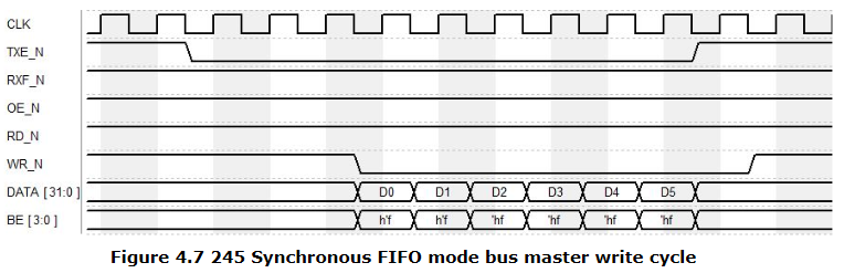
I wrote the FT6 Write block to work with the 245 Synchronous FIFO mode on the FT601 to write data to it. This was the simplest interface the FT601 offered, with only clock, data, and three control signals. When the PC requests data from the chip, TXE_N goes low (The host PC must poll the chip constantly to get a stream of data). The FT6 Write logic must then wait two cycles before taking WR_N low and sending the parallel data. The byte enable signal BE is always high since all the bytes need to be sent for maximum throughput.
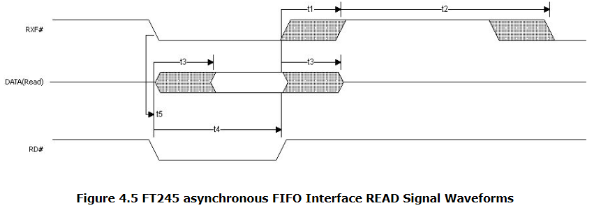
Moving on to the low-speed path, the module I started with was FT2 Read. The FT2232 offered a very similar interface to the FT601 with the option to forego a clock and operate asynchronously! I chose to use this asynchronous mode assuming it would be even simpler than the synchronous mode I used on the FT601. In a way I was right, all the FT2 Read block did was drop RD# low when RXF# was low, read a byte of data on the parallel pins, and pulled RD# high again. Then I encountered all sorts of timing issues since nothing was synchronized with the clock I was using (32 MHz, fed to the FPGA from an oscillator on the board). I didn't break out the pins needed to switch to the synchronous mode on the digital interface board, so I had to bandage together a fix on the FPGA. To do this, I ran the control signals through a synchronizer and clocked in the data based off of the now clock-synchronized signals. This worked, but still wasn't the most correct approach. I would recommend sticking to synchronous interfaces, and more importantly, routing out all the pins you can on the board so you don't lock yourself into a bad design decision.
The second FIFO in this design was a simple one. The input and output data widths were the same, and the read and write clocks were the same (making this a synchronous FIFO). I tried my hand at writing this one myself, which I did manage to do while searching madly through my old digital logic course notes! This FIFO allowed commands to be stored and then fed to the I2C/SPI transmit blocks in chunks of up to 256 bytes at a time, instead of the byte-by-byte flow of the interface from the FT2232.
Before starting to work on the SPI and I2C blocks, I made a breakout board for the digital interface and attached it to a logic analyzer so I could verify that I was sending data correctly. I used state machines to handle the logic behind these protocols as well as counters to divide the main 32 MHz clock into 8MHz for SPI and 400KHz for I2C. The first byte sent from the PC selects which protocol the rest of the data will be sent through. If SPI is selected, it configures a multiplexer for the SPI transmit block to send commands to either the front end or the ADC.
With all the FPGA code written, It was time for the moment of truth! In the next post I will explain how I tested the system as a whole, touch on the software needed to get the first bits of data out, and the bugs I uncovered once I got the data flowing!
Thanks for giving this post a read, and feel free to write a comment if anything was unclear or explained poorly, so I can edit and improve the post to make things clearer!
To stream the sample data as it comes it, it first needs to be converted into a format that the USB interface IC understands. USB interfaces generally come with specific applications in mind (e.g. USB to Ethernet, USB to SATA, USB to Camera Interface). If your application doesn't fit one of those niches, you must use one of the more general parts which typically use a 32-bit wide parallel interface. This is great for transferring any kind of data, regardless of protocol or type. However, our ADC does not have a matching 32-bit wide output. This means we need a device in between the ADC and USB interface to perform this conversion. A microcontroller would only take in data every clock cycle, which would require a blazing fast 1 GHz clock speed! A better choice for this task is an FPGA. These normally have a peripheral built in called a SERDES, which can take in very fast serial data and turn it into slower parallel data, acting as essentially a high speed shift register. FPGAs also have block memory which can be used to buffer the data so that small changes in transfer speed (caused by varying latency on the host PC) won't cause missing data. The FPGA can also take in commands from the USB interface and convert them to SPI and I2C commands to control the rest of the system.
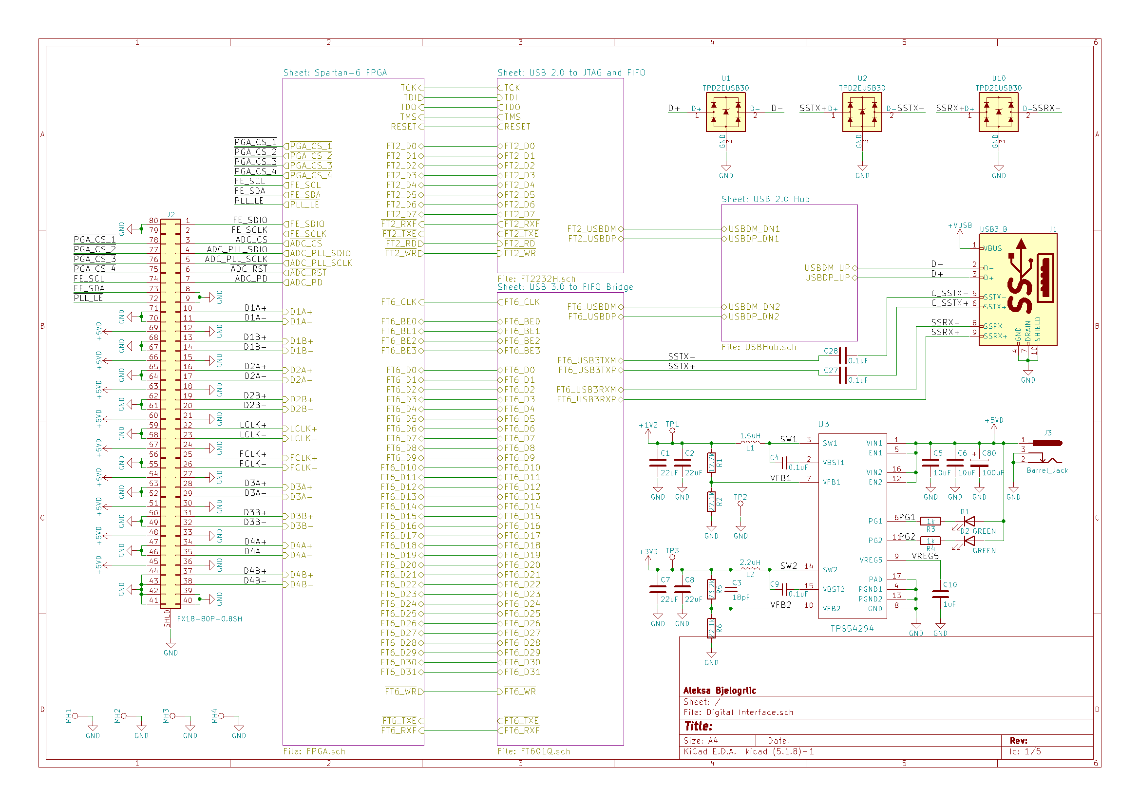
The main page of the schematic serves as a good block diagram for this board. The Spartan 6 LX4 FPGA from Xilinx was selected as it was the cheapest part that could handle the 1 Gbps LVDS inputs from the ADC. It also came in an easy to solder TQFP package and had just enough logic to do the basic tasks required of it, making it a perfect fit! I was going to use the Cypress FX3 line of USB interfaces, but I ended up switching over to the FT601 since it was a good deal cheaper and came in a QFN instead of a BGA package. This made it possible to inspect and fix soldering issues. I also read this excellent little whitepaper from Numato Labs which inspired me to use a separate USB 2 interface for side-band communication (like issuing serial commands to the rest of the board) and programming the FPGA. This whitepaper also had a neat trick up its sleeve: directly connecting the USB 3 RX/TX lines, while using a hub on the USB 2 connection! This saved me from using a USB 3 hub, lowering the cost and complexity of this board.
The numbers Mason! What do they mean? This was the first board that I added reference designators to, which are numbers that visually link parts on the board with their corresponding part on the schematic. This makes assembling and testing the board easier, as do the labels on the testpoints and LEDs. This was the first board I built for this project that I had a extra set of eyes on, which helped me catch some mistakes and improve the design as a whole. Huge thanks to my awesome co-workers at the time who reviewed the board with me!
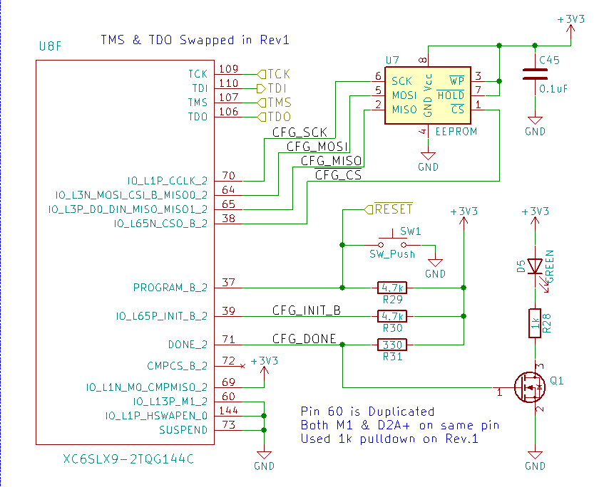
Unfortunately some issues always slip through, so don't put too much pressure on yourself to make Rev. 1 perfect! One such issue on this board was a classic pin swap - TMS & TDO on the JTAG interface to the FPGA were flipped. This made the FPGA impossible to program! It didn't even show up in OpenOCD, the software I was using to program it. I eventually fixed this by lifting both pins and soldering them to the opposite pads, a fix made possible by the TQFP package of the FPGA.
This didn't fix all of my programming woes, as for some reason the FPGA wouldn't load a bitstream from SPI flash. This meant I had to program it through JTAG every time it lost power, which made for an annoying development process. After searching OpenOCD documentation, reinstalling drivers, and pulling half my hair out, I finally looked back through my schematics and found the issue! I had accidentally given the same pin number to both a regular pin (which I was using to receive ADC data) and one of the boot mode select pins. KiCad had given the connection to the ADC priority over its direct connection to ground for setting the boot mode, leaving the pin floating during boot. I soldered on a pulldown to set the boot mode correctly, solving this issue.
The configuration block of the FPGA - basically the only pins that you can't swap!
Now that I could program the FPGA, I needed to learn Verilog to get it to do something useful. In my next post, I'll cover every block inside the FPGA, the things I learned starting to code in Verilog, and the mistakes I made along the way!
Thanks for giving this post a read, and feel free to write a comment if anything was unclear or explained poorly, so I can edit and improve the post to make things clearer. I'd also like to thank Hackaday and the Hackaday prize judges for selecting this project as a finalist for the Hackaday Prize, I'm very excited to continue to write about this project as I work to improve it further and hopefully make an awesome open source oscilloscope for everyone on their electronics journey!
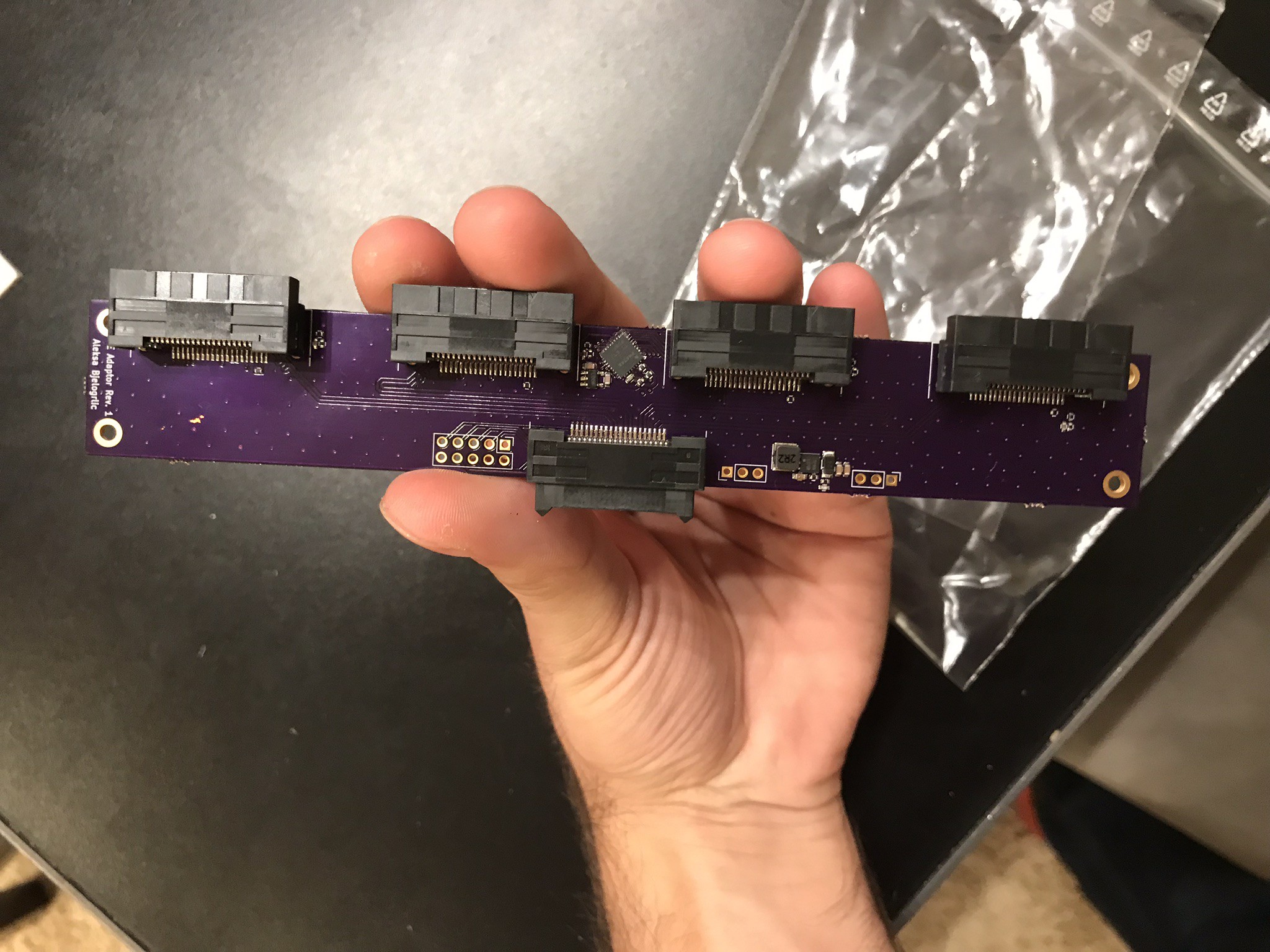
Before designing the ADC board, I made a separate adaptor board to take in four front end channels and bring them out to only one connector. This saved board area (and a lot of cost) by cutting down on the ADC board's width, giving the two boards a T-shaped profile.
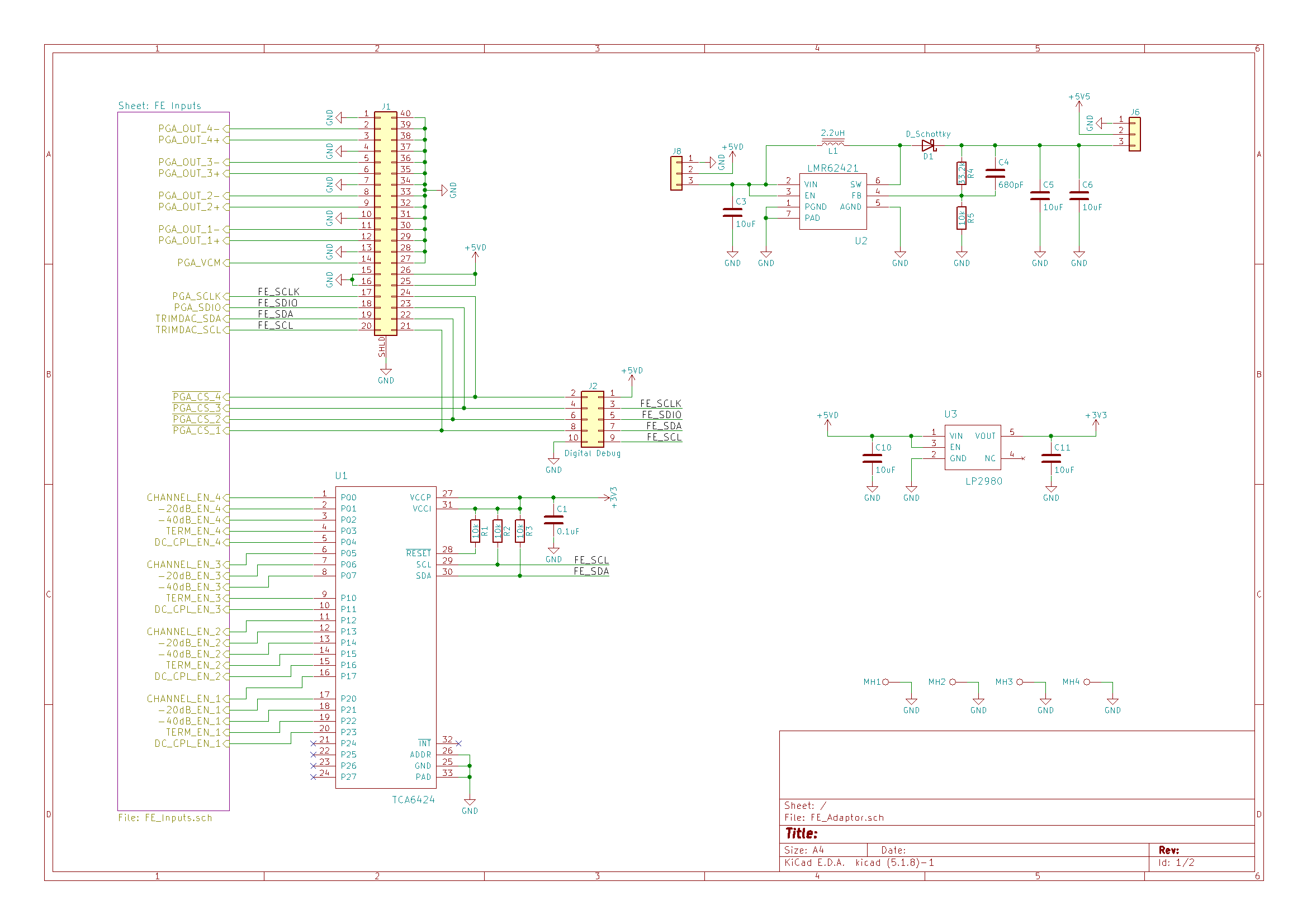
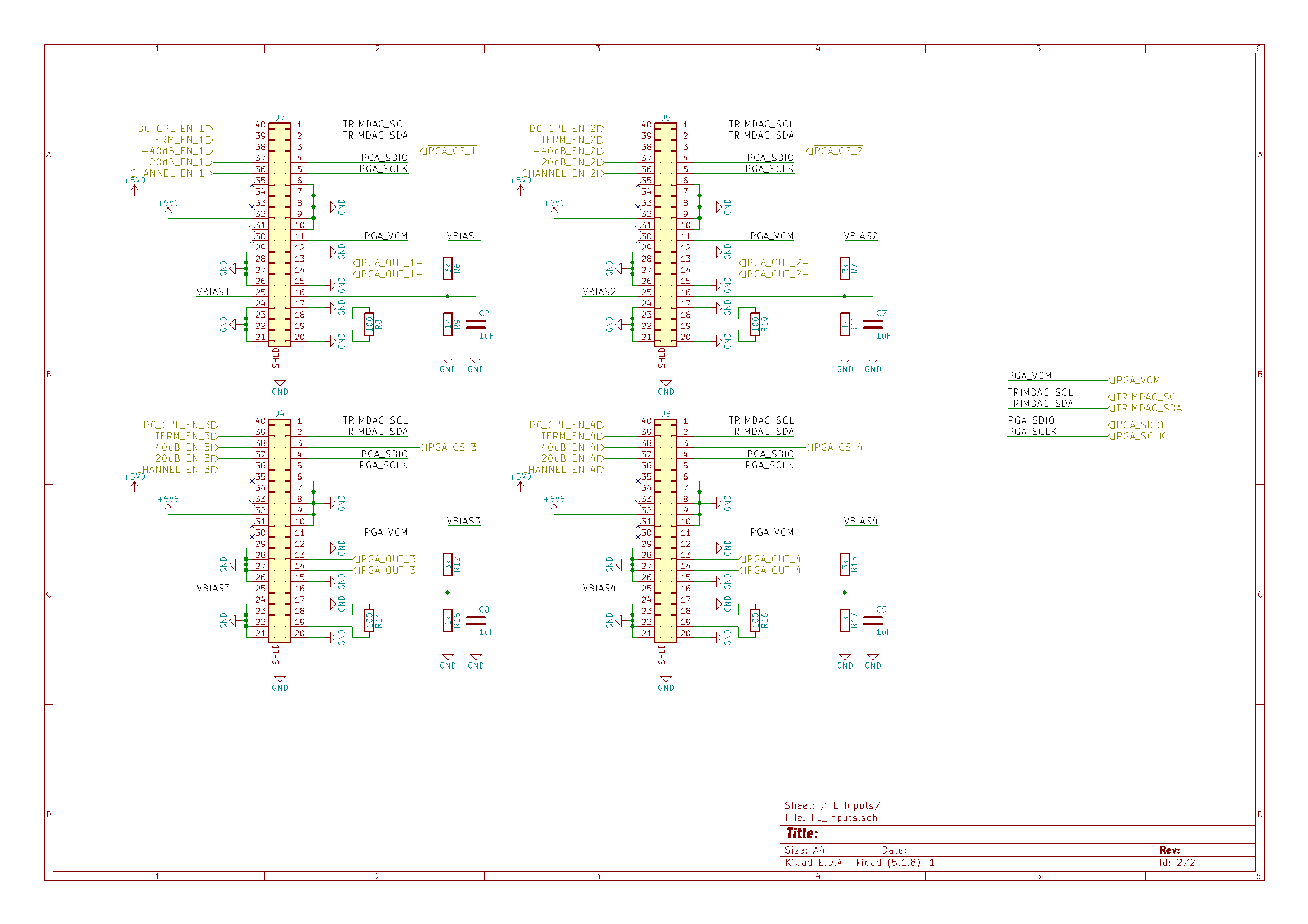
Each connection to the front ends terminated the unused AUX output of the PGA with 100Ω and set the AUX bias to mid-rail. The main outputs and bias input were routed to the ADC board connector (J1). As on the front end tester, the USB voltage was stepped up to 5.5V by a boost converter (U2) and both voltages were fed to each front end. The SPI and I2C interfaces were bused together (with separate chip selects for SPI) and routed to the connector for the ADC board as well as a debug connector (J2). An I2C GPIO expander (U1) was used to cut down on the number of connections to the rest of the system and a linear regulator (U3) was used to power it.
Live long and prosper, board. The poor thing almost didn't make it, since it was bigger than the hot plate I normally used to reflow solder boards with! But with enough hot air, the job was done.
ADC Board
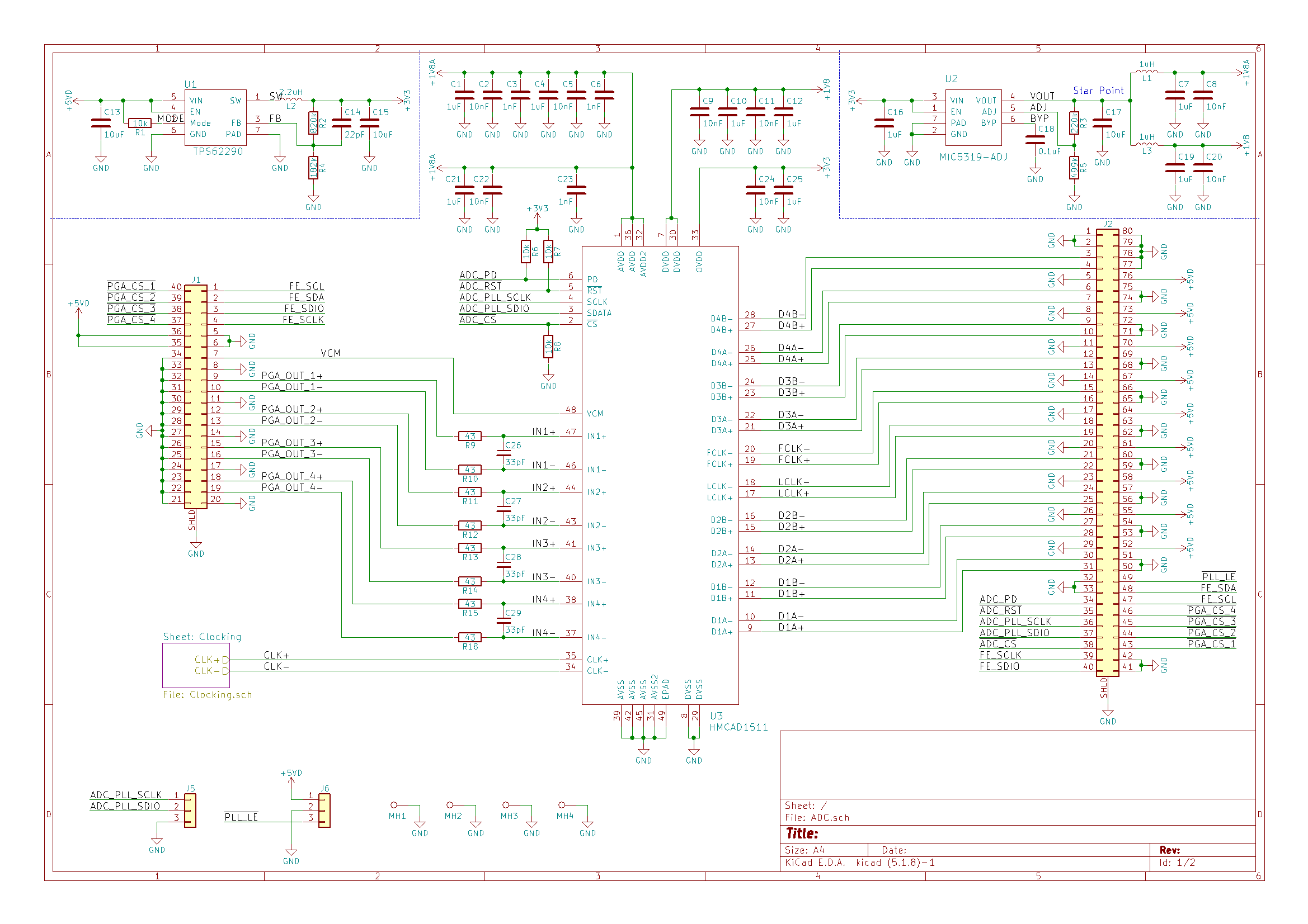
The HMCAD1511 ADC is an amazing little chip! I initially selected it since it was the cheapest 1 GSPS ADC I could find through normal distributors. Turns out, it has lots of tricks up its sleeve, like digital gain. This chip interleaves eight internal ADCs to sample one, two, or four channels at 1 GSPS, 500 MSPS or 250 MSPS respectively. Taking Nyquist into account (with some wiggle room for filtering), this allows for 350 MHz bandwidth on one channel, 200MHz on two channels, and 100 MHz on four channels. Sampled data is output on eight DDRLVDS lanes, with a bit clock and a frame clock for synchronization. Since no line operates faster than 500 MHz, this type of output requires no special high speed transceivers, making it easy to interface with a low cost FPGA. All of these factors explain why this ADC is also used on almost every low-cost oscilloscope on the market!
A step-down (buck) switching regulator (U1) was used to provide the 3.3V low-speed digital IO voltage and feed the linear regulator (U2) supplying the more sensitive analog and digital 1.8V rails. To prevent digital noise in the analog rail, two ferrite beads were used on each rail and connected to the output of the regulator at only one point (star point). For the decoupling caps, I generally try to meet or exceed whatever the evaluation board uses. I made another common mistake here and put a pull-down (R8) on the active low chip select line, instead of a pull-up. This meant the chip was always selected and listening for commands on the SPI bus... doh! Another mistake I made here was using the datasheet recommended input termination (R9,C26,R10) instead of the 100Ω that the PGA expects, resulting in a weird frequency response when I tested the system as a whole (but I'm jumping too far ahead here!). I added headers (J5,J6) and RF input connectors (J3,J4) to accommodate a clock generation module that I would design later. I chose to do this to avoid designing one circuit for the ~350MHz that the first prototype would need (at USB 3 Gen 1 speeds) and then another at 1GHz for the final prototype (at USB 3 Gen 2 speeds). To be able to use an external clock generator in the meantime, I added an SMA input (J7) that fed a balun (XFMR1) to provide the ADC with the differential clock input it needed. This input was DC-biased to mid-rail by the components on the CLK_VCM net.
Loads of pretty squiggles on this one! They're pretty functional too, as they strategically add extra length on some lines so that every signal gets to its destination at the same time, preventing potential timing issues. Aside from that, that big connector on the right connects to the last board in the chain (this project's grand finale?... not even close!), the digital interface. This board can't be tested until the digital interface is built, so fingers crossed it all works!
Thanks for giving this post a read, and feel free to write a comment if anything was unclear or explained poorly, so I can edit and improve the post to make things clearer!
To evaluate the front end as a whole, I made a tester board for it. This board brought out the analog outputs from the PGA to SMA connectors and included a socket for a Teensy (microcontroller dev board, similar to an Arduino nano) to interface with the PGA, DAC and control signals.
Aside from those main tasks, this board also stepped up the USB voltage to 5.5V, which was regulated back down to 5V for the PGA. This was done because USB VBUS voltage can drop as low as 4.75V, which is the minimum operating voltage for the PGA. When a linear regulator is added to "clean up" the voltage rail, the regulator's dropout voltage could cause the output to be below 4.75V, which the PGA isn't specified for. The common mode voltage for the PGA is also set on this board, for some reason I set this to 1.25V instead of the 0.9V needed for the ADC, but luckily enough I added an option to use the Teensy's DAC to set the voltage instead. In a classic blunder, I reversed the order of the GPIOs on the connector, but this could be flipped back in code.
Did I specify the Teensy just because I could get it in matching OSHpark purple? Yes, yes I did.
With all the boards connected, the tests could begin! As expected, the PGA (with its 900 MHz of bandwidth!) didn't impact the frequency response much. However, I noticed a flaw in my plans for the overall system when testing the values from my spreadsheet.
Although the PGA was supposed to drive the ADC directly with about 1.8V full scale, it wasn't able to drive more than 0.9V at higher gains!
This was, of course, in the datasheet! Tempted to repeat the mistake I made with Rev. 2 of the FFE board, I frantically scrambled to think of a solution. I looked for an ADC driver with enough gain to allow the PGA to output the 0.7V it was actually designed for, and give the ADC the 1.8V it needed. But having learned my lesson at that point, I took some time to really read over the ADC's datasheet. I found out it had built in digital gain that could be used for this task! The ADC actually samples at a higher than 8-bit resolution internally, so at low gains (in this case, ~2.5x) this feature had very little cost to overall performance, as the resolution with the gain applied was still greater than 8 bits. This enabled an entirely new architecture for the FFE! Until then, I elected to continue designing the rest of the system before going back to make the new front end. Next up, the ADC board!
Thanks for giving this post a read, and feel free to write a comment if anything was unclear or explained poorly, so I can edit and improve the post to make things clearer!
If the FFE is the front of the front end, then what's in the rest of the front end? To complete the front end, this board needed finely adjustable gain, dc offset control, nyquist filtering, and an ADC driver. That sounded like a lot of work! Luckily enough, [bunnie & xobs'] probe schematics introduced me to just the right part for the job, the LMH6518 PGA. With adjustable gain from −1.16 dB to 38.8 dB, a whopping 900 MHz bandwidth, selectable bandwidth limit and 100Ω differential output, this chip had it all!
To use the input signal from the FFE with this chip, it had to be level shifted from +/-2.5V to 0-5V to fit within the PGA's positive voltage range. This was done by a pair of resistors (at the cost of a 2x attenuation!). DC offset control was accomplished by feeding a DAC output into one end of the PGA. This board also forced me to standardize on a connector series to use for the rest of the prototype. I ended up going with the FX18 series from Hirose, as they were compact (with a reasonably solder-able 0.8mm pitch), rated for high speeds, and had right-angle options that allowed me to connect everything in one plane.
The QFN package gave me some trouble and required rework later, but otherwise this board came together pretty well. I didn't want to continue on with the next board down the line without making sure this chip worked as expected, but probing that connector or its pins would be awful. And so we move on to the topic of the next post, making a front end tester board and testing the front end as a whole!
Thanks for giving this post a read, and feel free to write a comment if anything was unclear or explained poorly, so I can edit and improve the post to make things clearer!
Now that FFE Rev 1 was built, I had to test it to see if it met the lofty goals I set for it in my front end specs - 350MHz bandwidth, 1MΩ//15pF input impedance, 4 selectable attenuation ranges (0x,10x,100x,1000x), AC/DC coupling and switchable 50Ω termination.
*Spoiler Alert* It did not.
And that's fine, it was my first revision and that was pretty much to be expected. This log details how I tested it and the things I learned along the way!
Test Setup
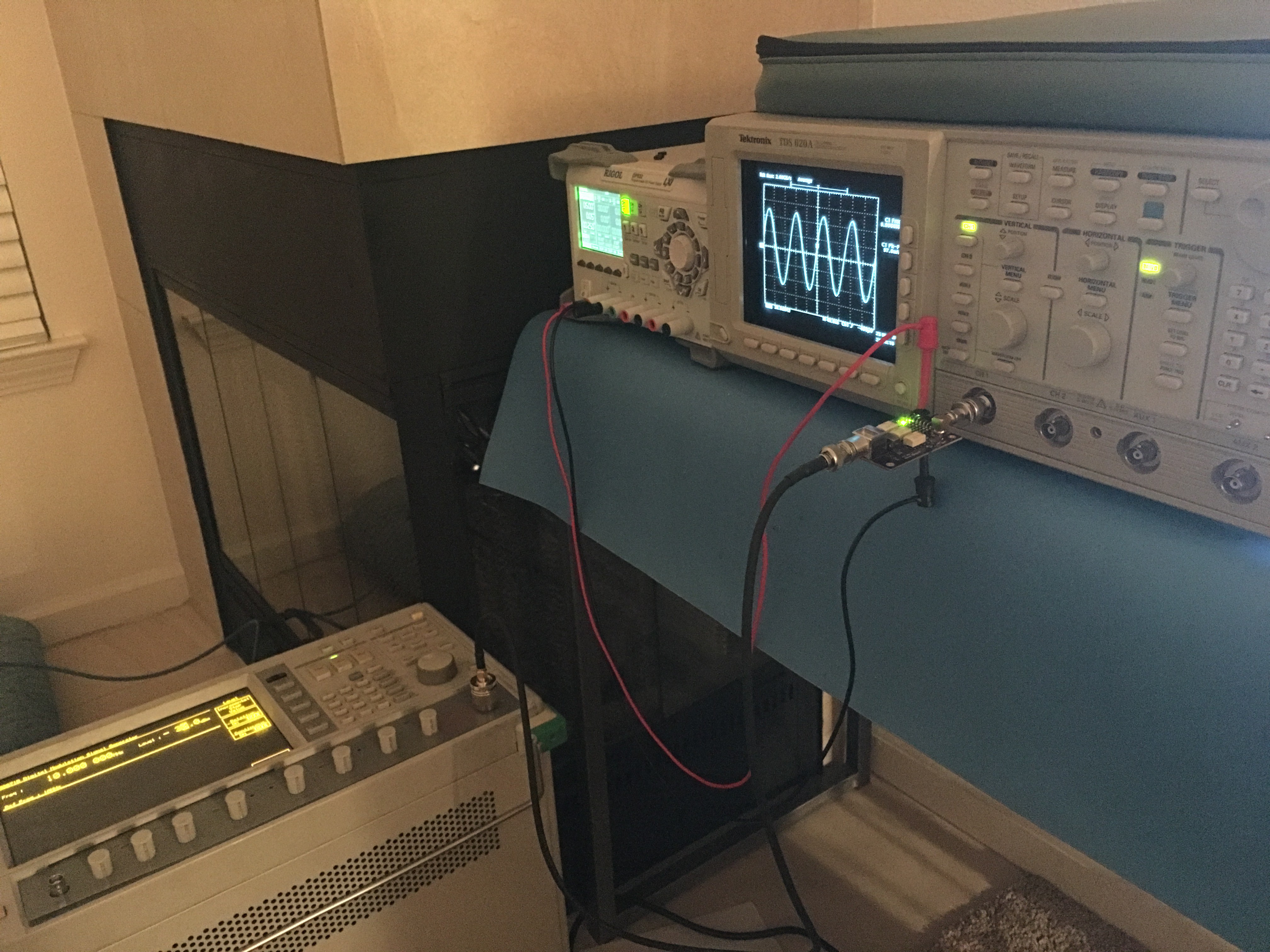
After annexing a corner of the living room (with apologies to my housemates), I set up a power supply, oscilloscope, and RF signal generator to start frequency response testing on the FFE board. I swept frequencies with the signal generator and recorded the average amplitude off of the oscilloscope. This got tedious very quickly, but I eventually automated it with a USB GPIB controller and PyVISA. GPIB is just about as old as dirt, but if you happen to have equally as old equipment, it's an absolute lifesaver.
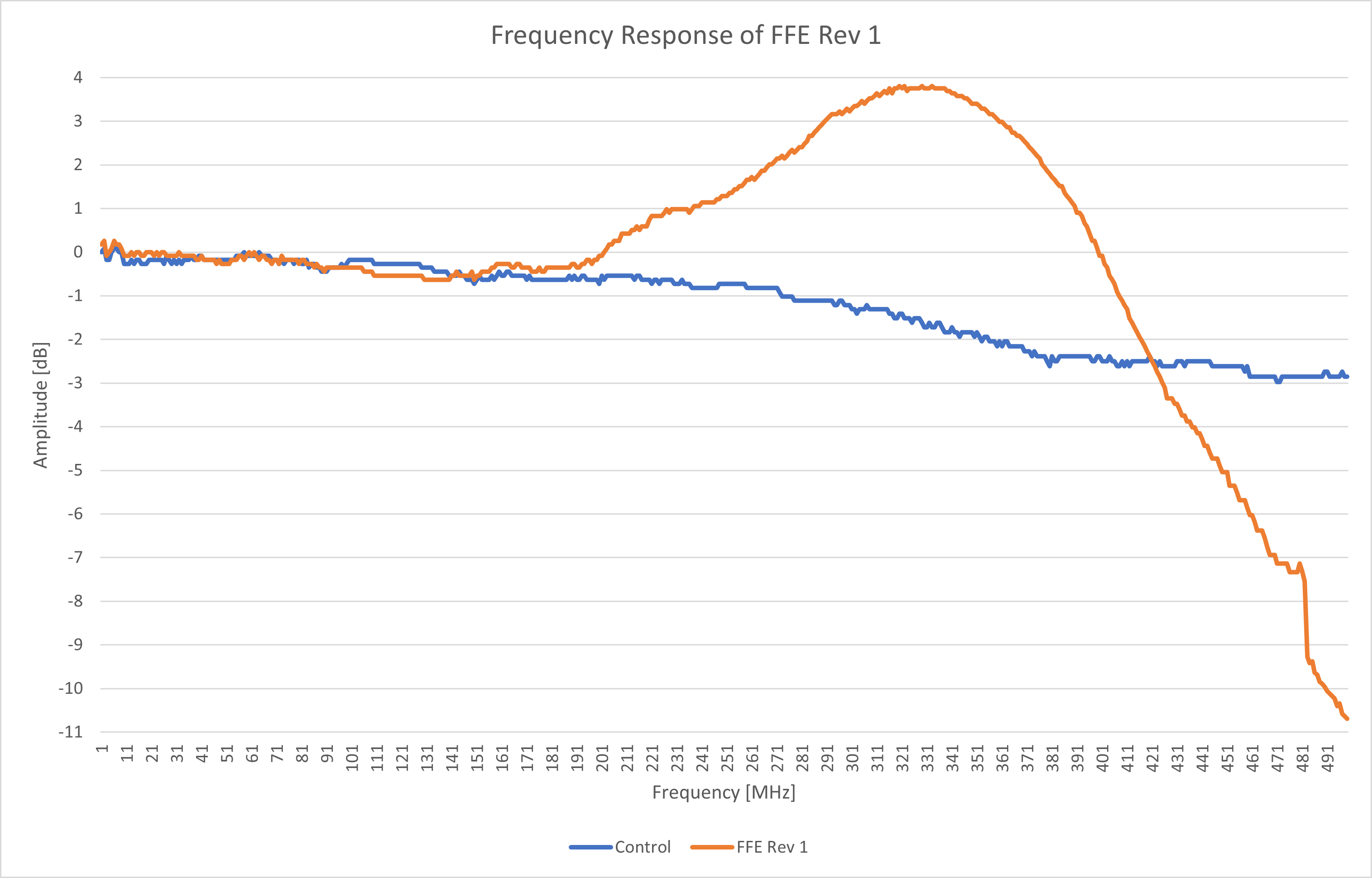
Here's the frequency response of FFE Rev 1 with the attenuators off, AC coupling on, and 50Ω termination enabled. The blue line is the frequency response of the oscilloscope doing the measurements to provide some sort of baseline for relative comparison (my equipment wasn't calibrated, so technically relative measurements are all they're capable of). Although the -3dB bandwidth was over 400MHz, there was massive (3db!) peaking past 200MHz. This wouldn't work for a front end. On top of that, the output oscillated from rail to rail when any of the the attenuators were enabled. The only good news was that it worked with regular scope probes.
The reason for the peaking eluded me at the time, though now I believe it was due to either the opamp's marginal stability at a gain of ten or the parasitic inductance and capacitance in the layout, perhaps even both. When filtered by the PGA's adjustable bandwidth limit (I would set it to 200MHz), I thought that the peaking would be acceptable enough to test the rest of the system until I made a new revision. As for the attenuators, switching them in massively increased the capacitance at the opamp input, which was probably the cause of the oscillation. I'd have to avoid using them whenever testing the system, which limited me to a select few voltage ranges.
Rev 2
It really bugged me to move on to designing the rest of the system while the FFE was still an absolute mess! Instead of scrapping the design and figuring out the fundamentals behind why it didn't work, I came up with a solution in a single afternoon (this had to be good right?). The idea was to take some of the pressure off of the main opamp, and add another one in front of it to better handle the changing capacitance when the attenuators switch.
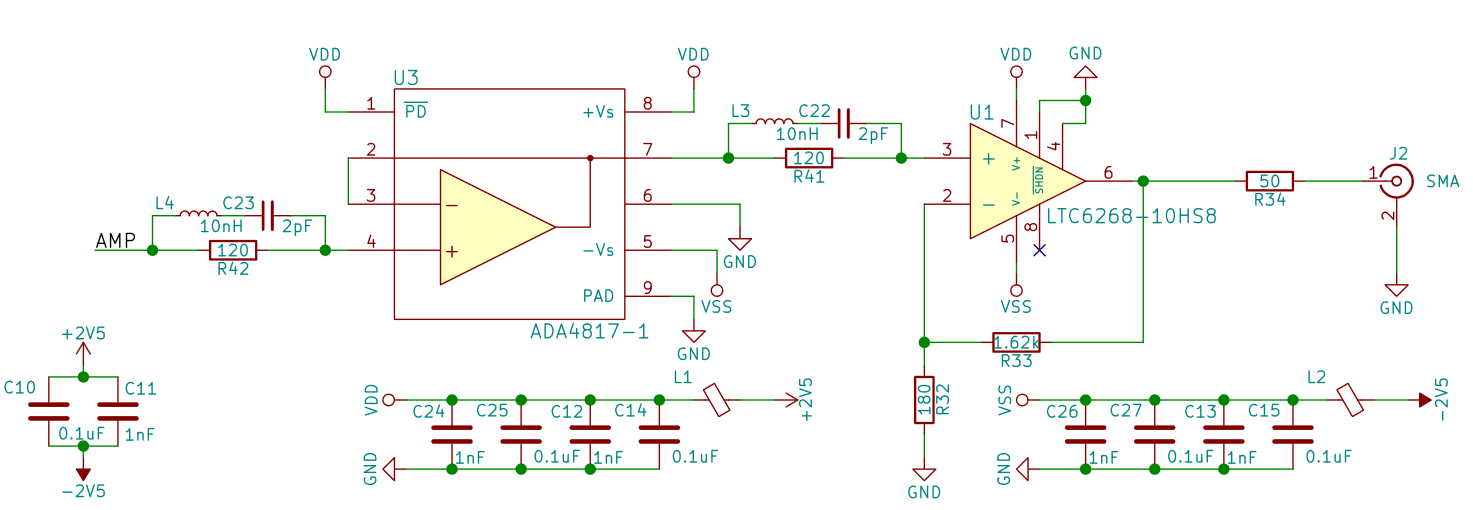
I used the same ADA4817-1 opamp that [bunnie & xobs'] used in their oscilloscope probe, alongside the damping circuit (which they DID label as damping 1GHz peaks, so I figured tweaking the values would help me tame the mountainous peak at 340MHz). So in the same afternoon that I thought of this fix, I layed it out and sent it off to fab!
The only thing that's peaking here is the BOM cost with the extra opamp! Kidding aside, it was clear that the FFE was going to be very difficult to do right, and would need a complete overhaul for Rev 3. Until then, I would continue to build the rest of the system so that work on software could start, and then loop back and give the FFE the respect it's due.
Thanks for giving this post a read, and feel free to write a comment if anything was unclear or explained poorly, so I can edit and improve the post to make things clearer!
An oscilloscope's input buffer has a very odd (and strict) set of requirements. Its input impedance must be 1MΩ in parallel with about 15pF, for compatibility with standard oscilloscope probes. The front end must also take in any signal within the oscilloscope's voltage ranges and attenuate or amplify it to fit the ADC full-scale voltage. It must be able to AC or DC couple the input signal as well as terminate it in 50Ω (on higher end scopes). On top of these requirements, the front end must keep voltage noise low enough to be undetectable by the ADC as well as meeting a maximum bandwidth of 350MHz!
Rev.1
Once again taking inspiration from [bunnie & xobs'] oscilloscope module (specifically the probe schematics) I decided to use an opamp to provide the high impedance, high bandwidth part of the buffer. To spec this opamp out, I had to know what gain I needed for the system. I wanted to find the minimum gain I needed, so I used the lowest full-scale voltage on the ADC, 1.8V. I divided this by the input voltage at the lowest voltage range. I wanted the scope to be capable of 500uV/div, which with 8 divisions gives an input voltage of 4 mV peak to peak. Therefore, the maximum gain of the system was 1800mV/4mV = 450 V/V. That's a lot of gain! And since I used the resistor level shifting from the linked probe schematics, I had to double the gain to offset the resistive losses. So out of 900 V/V of gain, the PGA I wanted to use provided about 87 V/V maximum, leaving about 10x gain left for the poor buffer opamp to squeeze out. With a desired bandwidth of 350MHz, the opamp needed a gain bandwidth product of over 3.5GHz! It also needed a high impedance input, very low noise and a blazing fast slew rate.
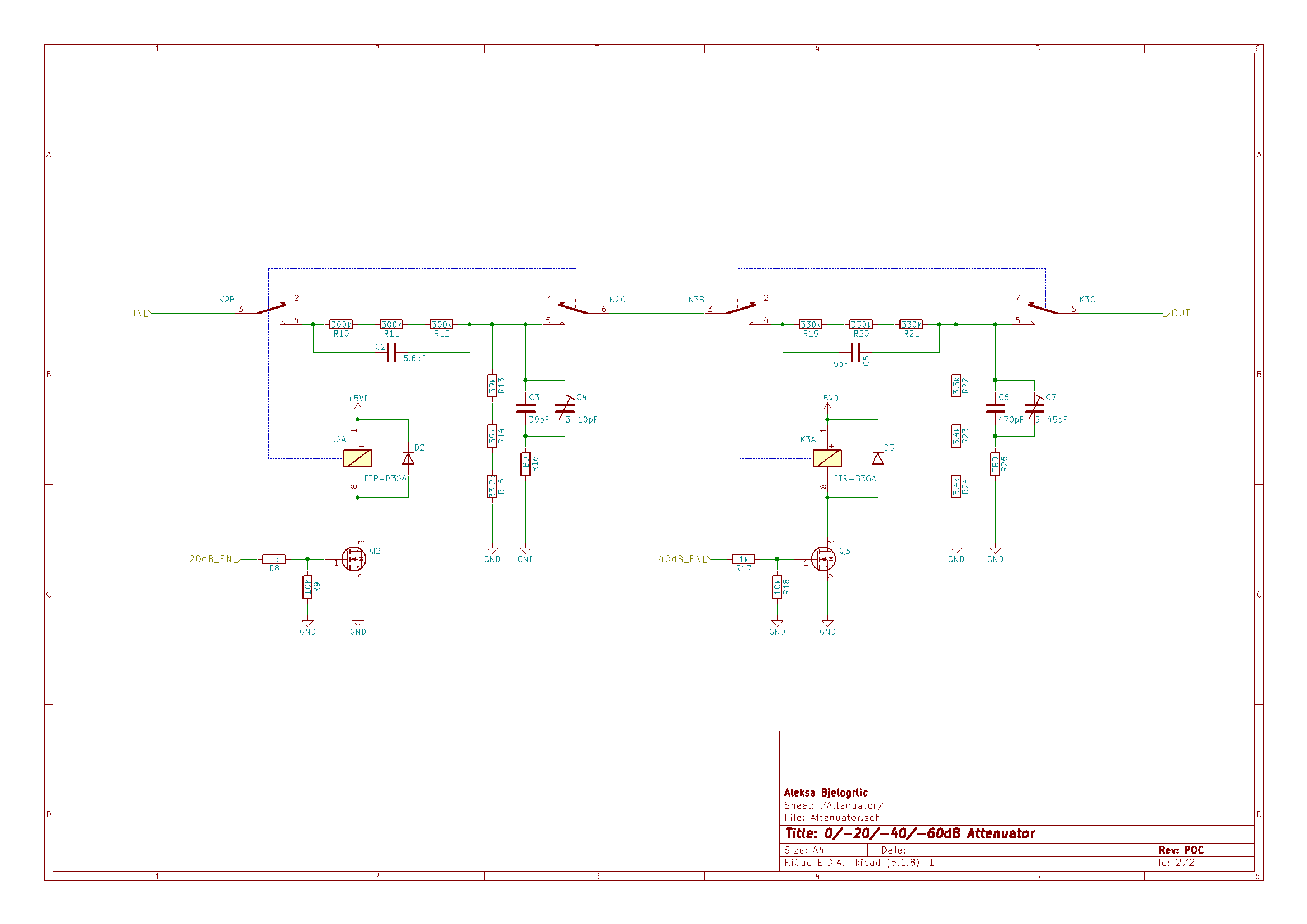
A parametric search left me with only one opamp that was up to the challenge, the LTC6268-10. This ticking time bomb of BOM cost had a few drawbacks other than the price tag. First of all, this part is a "de-compensated" opamp that requires a minimum gain of 10 for stability. Since a gain of 10 is needed, this is just barely stable. Second, due to the slew rate, the output voltage must remain under 0.45V peak to peak to avoid distortion due to slewing. Combining these two, the maximum input voltage was 0.45/10 = 0.045V. To work with this limitation, I designed a system of two attenuators to give 10x, 100x, and when combined, 1000x attenuation. Shown below is a spreadsheet of all the voltage ranges and how the attenuators and programmable gain amplifier (PGA) needed to be configured to meet the ADC's lowest full scale voltage of 1.8V.
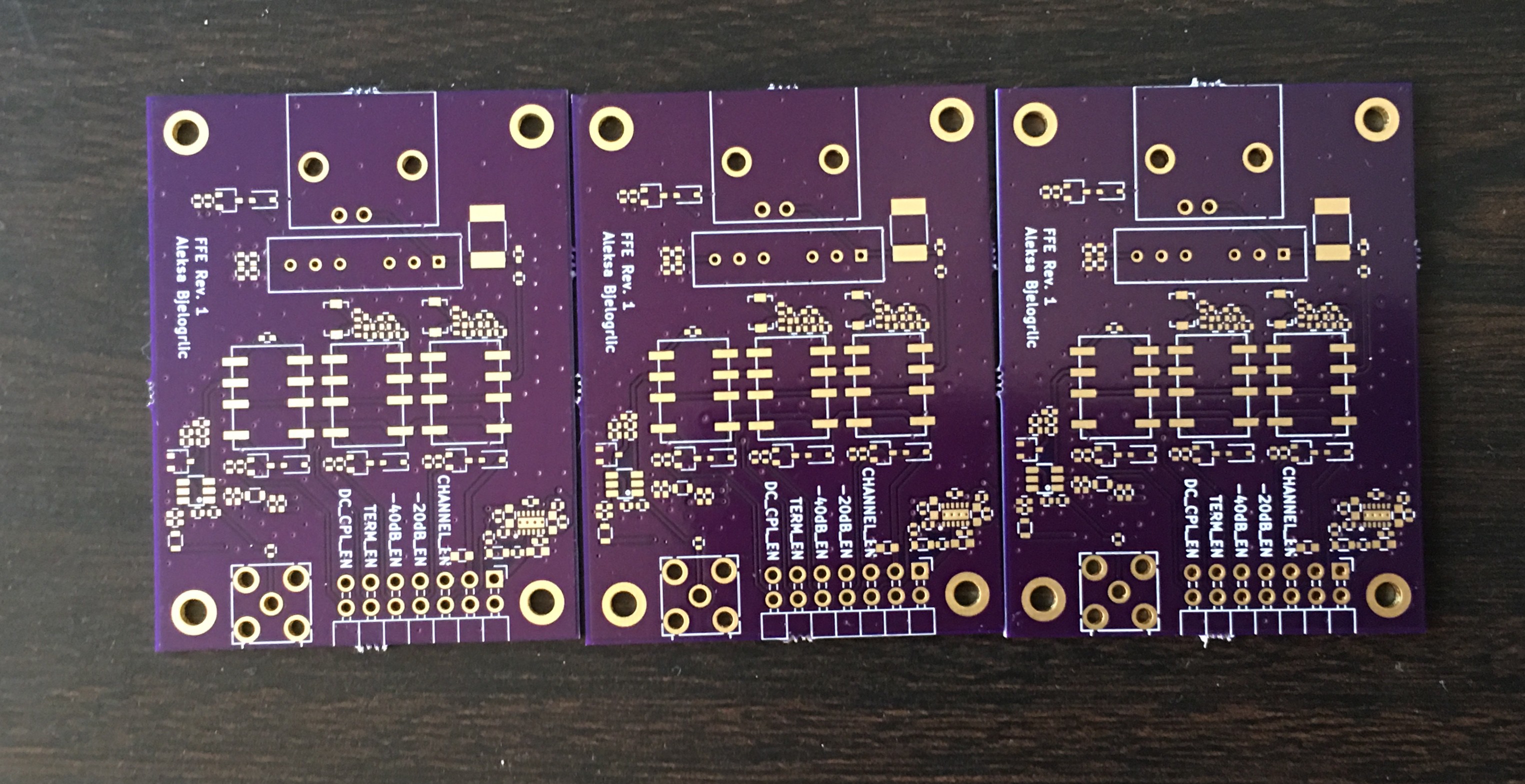
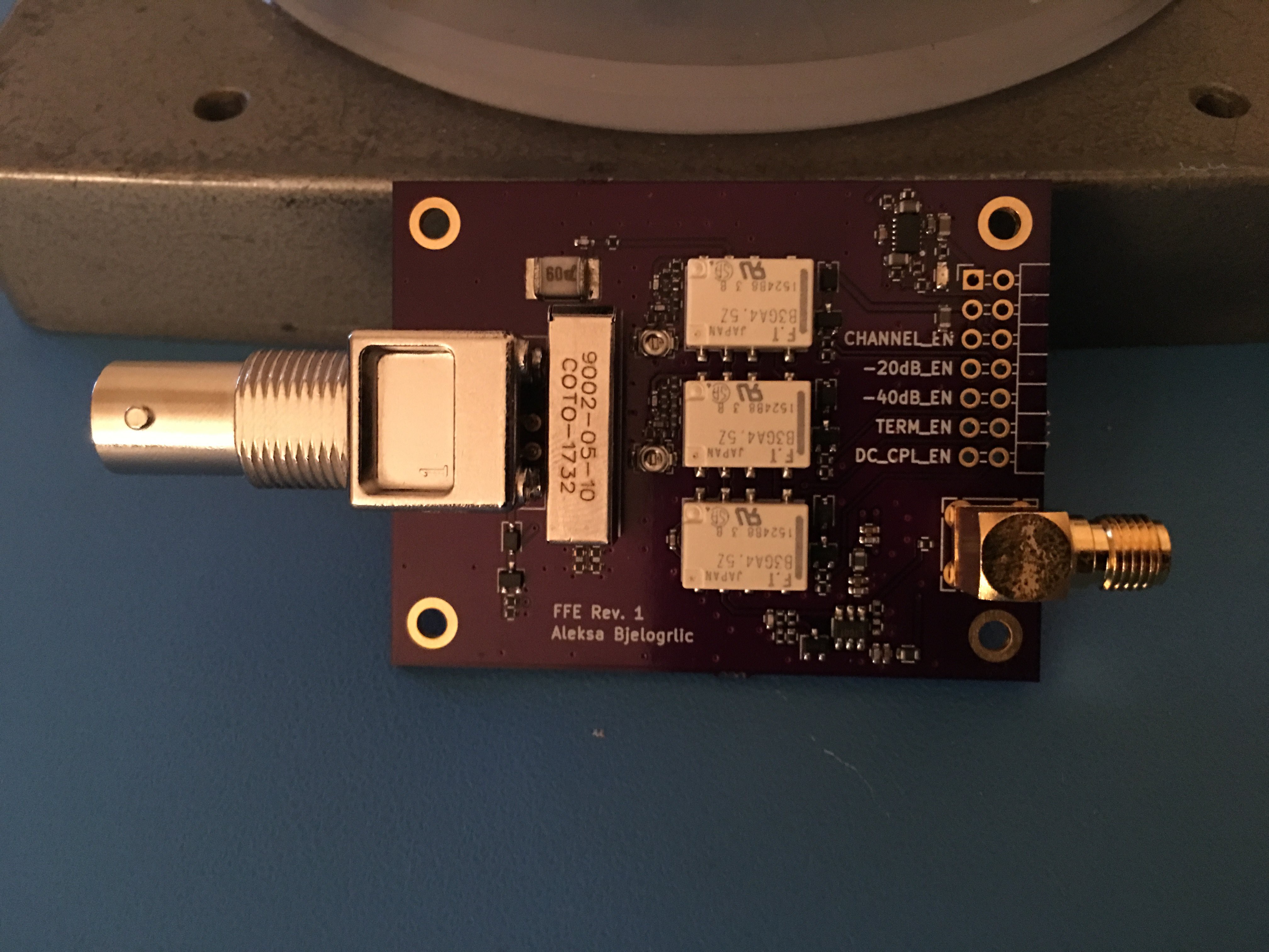
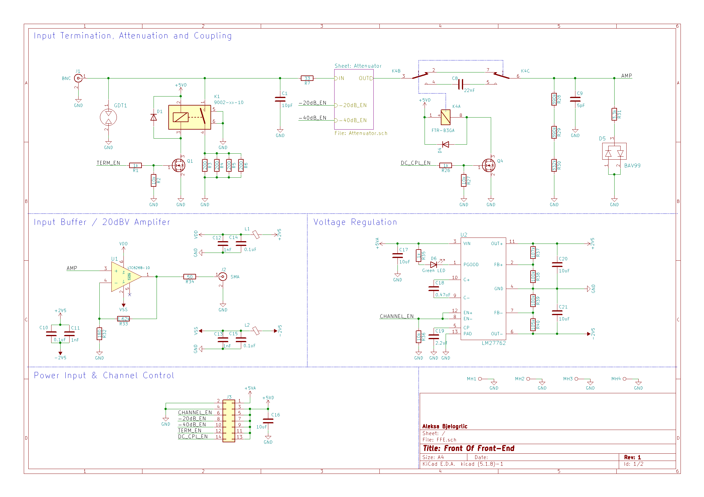
With the opamp chosen, and all these requirements in mind, I booted up my trusty copy of KiCad 4 (I wasn't a Luddite, that was the latest version then!) and got to work. Below are the schematics of the first revision of the FFE. The gas discharge tube (GDT1) provides some degree of input protection, while the reed relay (K1) provides the switchable 50 ohm termination. C1 and C9, alongside R28-30, provide the required 1MΩ//15pF input impedance when the attenuators are off. The attenuators are compensated voltage dividers designed to present the same impedance (1MΩ//5pF) as C9//R28-30 when switched on or off by the relays. R7 should really have been in front of D5 and R31 removed in order to provide protection to the opamp input without adding series resistance that risks lowering the bandwidth of the system. The K4 relay provides selectable AC or DC coupling by switching C8 in or out of the circuit. The opamp circuit is an amplifier in a non-inverting configuration, with a 50Ω output impedance, set by R34, and a SMA output for direct connection to equipment for testing. The LM27762 was used to generate clean positive and negative rails (an integrated LDO cleans up the noisy output from the charge pump used to invert the input). Finally, a right angle 2x7 header connects the various enable signals to the upcoming PGA board, while allowing manual tests to be conducted with jumpers.
From perfect purple PCBs to potentially performant prototype - thanks to OSHpark's four layer service, aluminium stencil from OSHstencils, and an afternoon under the microscope! At the time this photo was taken, I either ordered the wrong headers or forgot to order them entirely, but who manages to make only one order for a board anyway? In my next post, I'll discuss this revision's test results, problems encountered, and a hasty band-aid solution that proved I should always get a good night's sleep before sending out a new board!
Thanks for giving this post a read, and feel free to write a comment if anything was unclear or explained poorly, so I can edit and improve the post to make things clearer!
The origins of this project lie in [bunnie & xobs'] excellent Novena project, which came about around the time I first became interested in hardware. The Novena had an FPGA co-processor tightly coupled to its CPU, which was used alongside a high speed ADC and a front-end (housed INSIDE a probe!) to make an oscilloscope module. This, alongside much aspirational viewing of [Dave Jones'] oscilloscope reviews and tear-downs, got me thinking about designing an oscilloscope myself.
Software Defined?
After bouncing some ideas off of my friends at university, I became convinced it would be possible to transfer every sample from the ADC to the user's computer in real time, with all the triggering and processing being done by the CPU. This would offer huge advantages compared to regular benchtop scopes! Your sample memory would only be limited by the amount of RAM on your computer, as opposed to the piddly 24 Mpts on scopes such as the ever-popular Rigol ds1054z. Waveform update rate could exceed the 1 million waveforms per second offered by Keysight's InfiniiVision series since processing is done on a modern multi-core CPU, unrestrained by BOM cost limitations on FPGAs or by the fixed nature of ASICs. Speaking of BOM cost, by not having to pay for any real processing, memory, display or power supply, this design can be made competitively to other low cost scopes. This savings also allows for a more capable front end, allowing you to get the most of the 1Gs/s ADC by offering 100 MHZ bandwidth on four channels, 200 MHz on two channels, and 350 MHz on a single channel.
Block Diagram
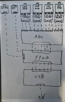
Here was my initial sketch of the design in March 2018. Sorry for the poor resolution, I knew the photo existed somewhere, but could only find a thumbnail file!
You can see the influence from the Novena oscilloscope module in planning to use all those SATA connectors and in the choice of PGA. The idea was to make the whole system modular, so that each part of the scope could be tested individually. From left to right at the top, we have an external trigger, 10KHz probe compensation, and a module for each channel labeled FFE, for Front of Front End. These modules would hold the input buffer for the next module down the line, the Programmable Gain Amplifier (PGA). This would drive the ADC inputs, and the ADC would connect to the FPGA. The FPGA would handle the external trigger, probe compensation, and convert the ADC's output into something the USB interface could understand. Finally, the USB interface would send all the data to the user's computer.
At the time, there were USB 3 Gen 1 (5 Gbps) interface ICs available and the faster Gen 2 ICs were promised to be in the works. So a Gen 1 chip was chosen with the plan to migrate to Gen 2 when the ICs became available. The parts linked were the ones chosen at the time, so stay tuned for the individual posts for each of the blocks above! Except the external trigger, I dropped that almost right after making this block diagram.
 Aleksa
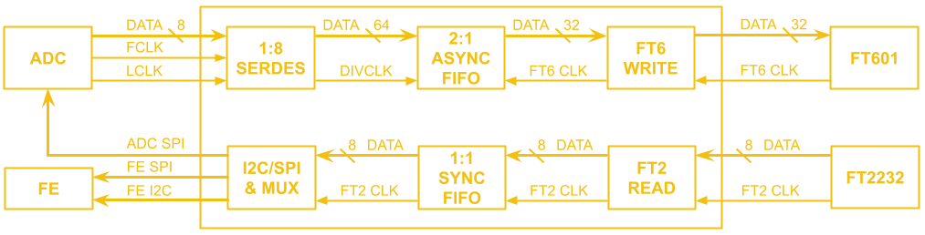
 The main page of the schematic serves as a good block diagram for this board. The
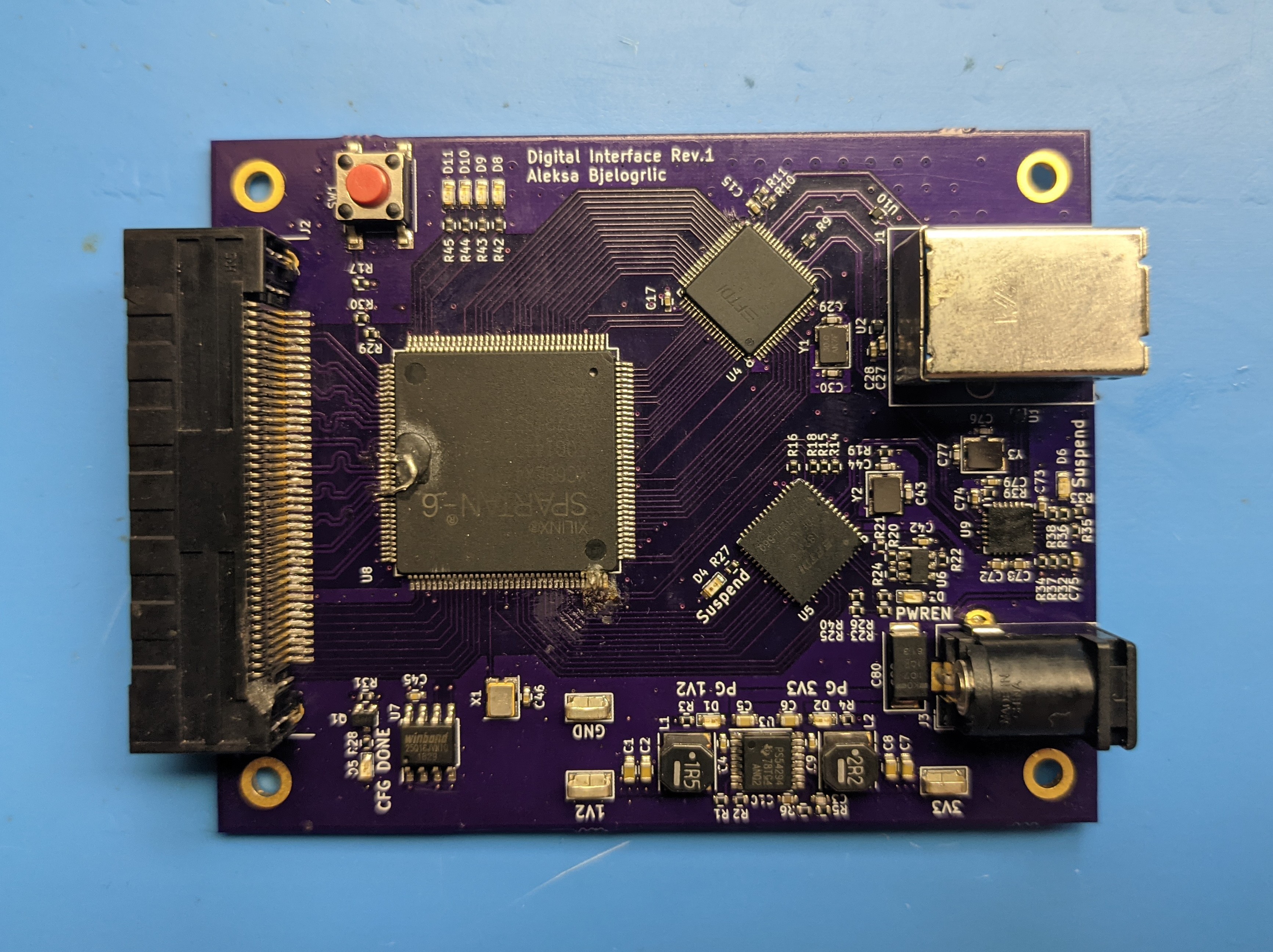
 A step-down (buck) switching regulator (U1) was used to provide the 3.3V low-speed digital IO voltage and feed the linear regulator (U2) supplying the more sensitive analog and digital 1.8V rails. To prevent digital noise in the analog rail, two ferrite beads were used on each rail and connected to the output of the regulator at only one point (star point). For the decoupling caps, I generally try to meet or exceed whatever the
 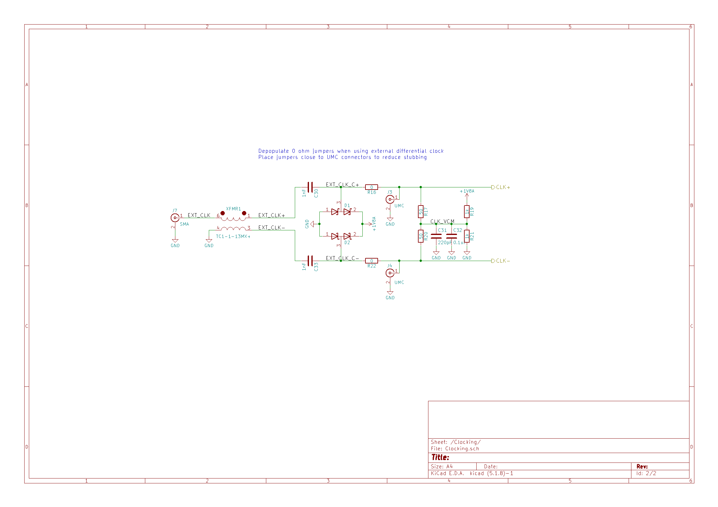 I added headers (J5,J6) and RF input connectors (J3,J4) to accommodate a clock generation module that I would design later. I chose to do this to avoid designing one circuit for the ~350MHz that the first prototype would need (at USB 3 Gen 1 speeds) and then another at 1GHz for the final prototype (at USB 3 Gen 2 speeds). To be able to use an
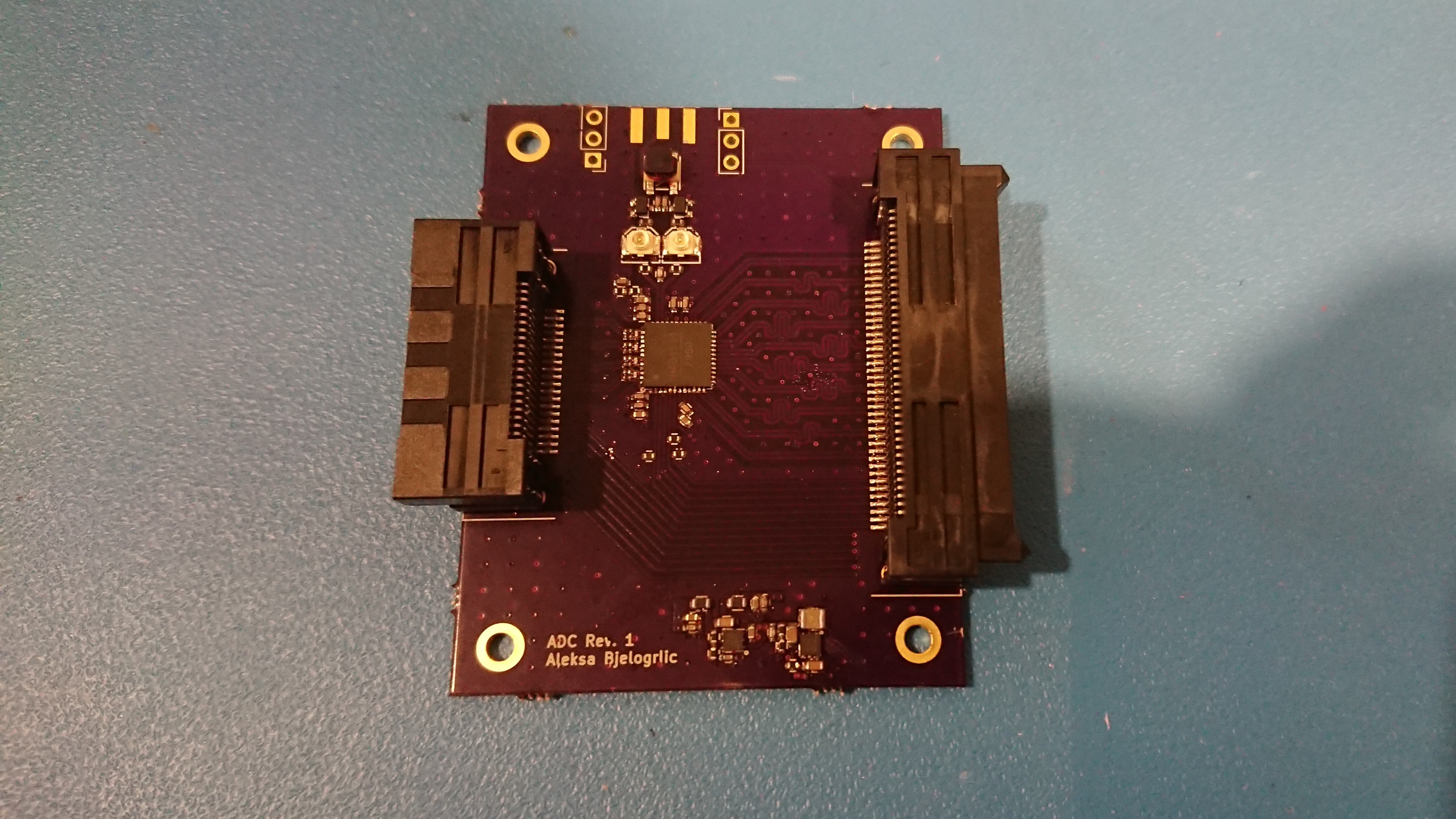
 Aside from those main tasks, this board also stepped up the USB voltage to 5.5V, which was regulated back down to 5V for the PGA. This was done because USB VBUS voltage can drop as low as 4.75V, which is the minimum operating voltage for the PGA. When a linear regulator is added to "clean up" the voltage rail, the regulator's dropout voltage could cause the output to be below 4.75V, which the PGA isn't specified for. The common mode voltage for the PGA is also set on this board, for some reason I set this to 1.25V instead of the 0.9V needed for the ADC, but luckily enough I added an option to use the Teensy's DAC to set the voltage instead. In a classic blunder, I reversed the order of the GPIOs on the connector, but this could be flipped back in code.

 Although the PGA was supposed to drive the ADC directly with about 1.8V full scale, it wasn't able to drive more than 0.9V at higher gains!
 This was, of course, in the
  To use the input signal from the FFE with this chip, it had to be level shifted from +/-2.5V to 0-5V to fit within the PGA's positive voltage range. This was done by a pair of resistors (at the cost of a 2x attenuation!). DC offset control was accomplished by feeding a DAC output into one end of the PGA. This board also forced me to standardize on a connector series to use for the rest of the prototype. I ended up going with the

 I used the same
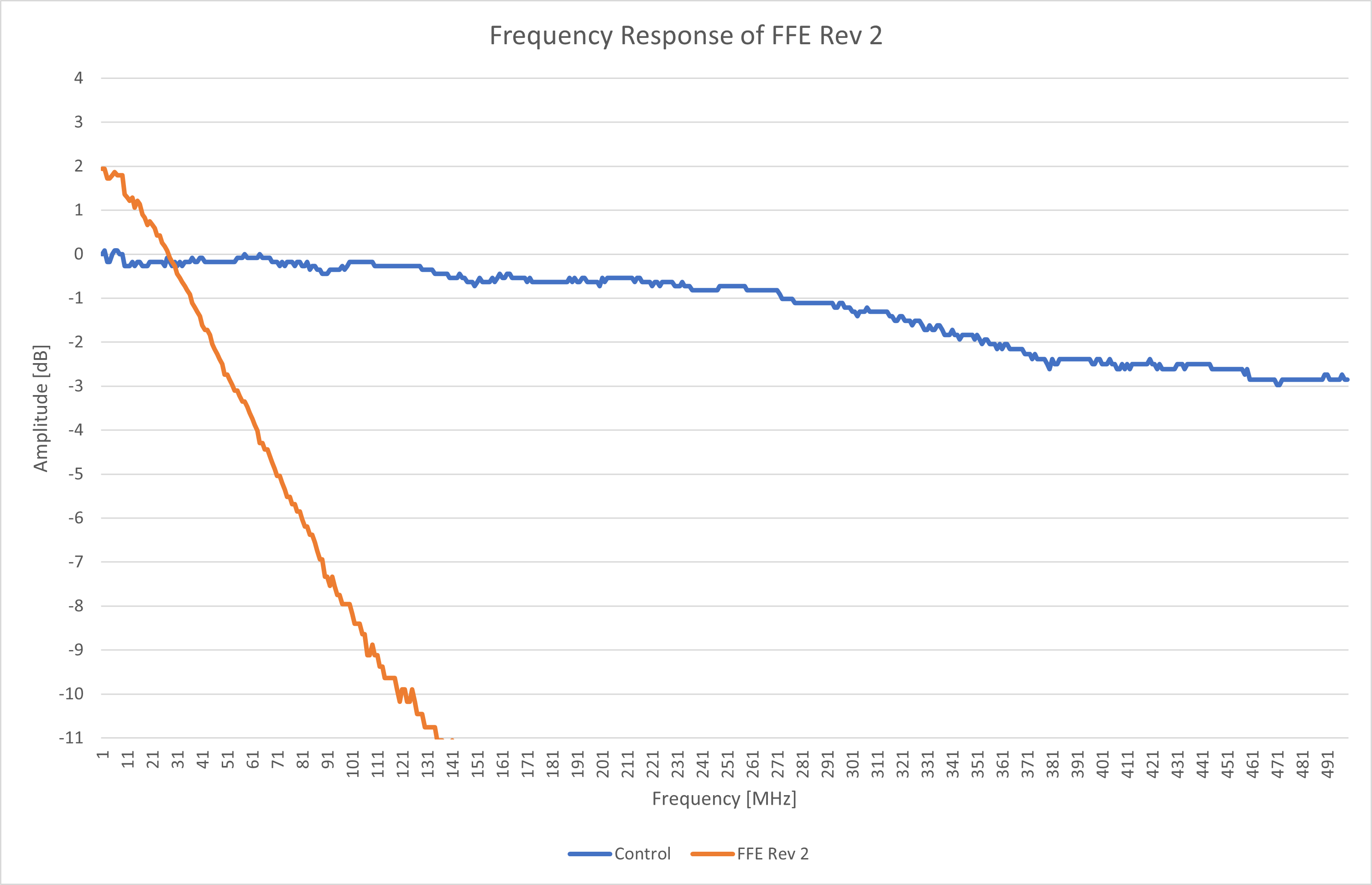
 The gas discharge tube (GDT1) provides some degree of input protection, while the reed relay (K1) provides the switchable 50 ohm termination. C1 and C9, alongside R28-30, provide the required 1MΩ//15pF input impedance when the attenuators are off. The attenuators are