Manu
ManuThe schematic is nothing special, a commonly used circuit for electronic loads. It's an op-amp that senses the voltage drop across a current shut ( in this case a set of resistors connected in parallel ) by having the feedback connected to the inverting input. A voltage reference ( TL431 ) is used to provide a reference voltage of 2.495v, which is wired to the non-inverting input. The output of the op-amp is connected to the gate of an N-Channel MOSFET ( IRFZ44N ).
Since the op-amp always tries to keep its inverting and non-inverting inputs the same, the output on the op-amp connected to the gate is always varied to generate a voltage drop across the current shunt that equals the reference voltage at the non-inverting input. That means with a voltage reference of 1 volt applied at the non-inverting input, a current of 1 amp will be drawn if the shunt resistor is 1 ohm. TL431 was used to reduce the temperature voltage drift and also since the voltage reference max out at 2.5v with a shunt of 1 ohm we can set a max current of 2.5A which is more than enough for most conditions.
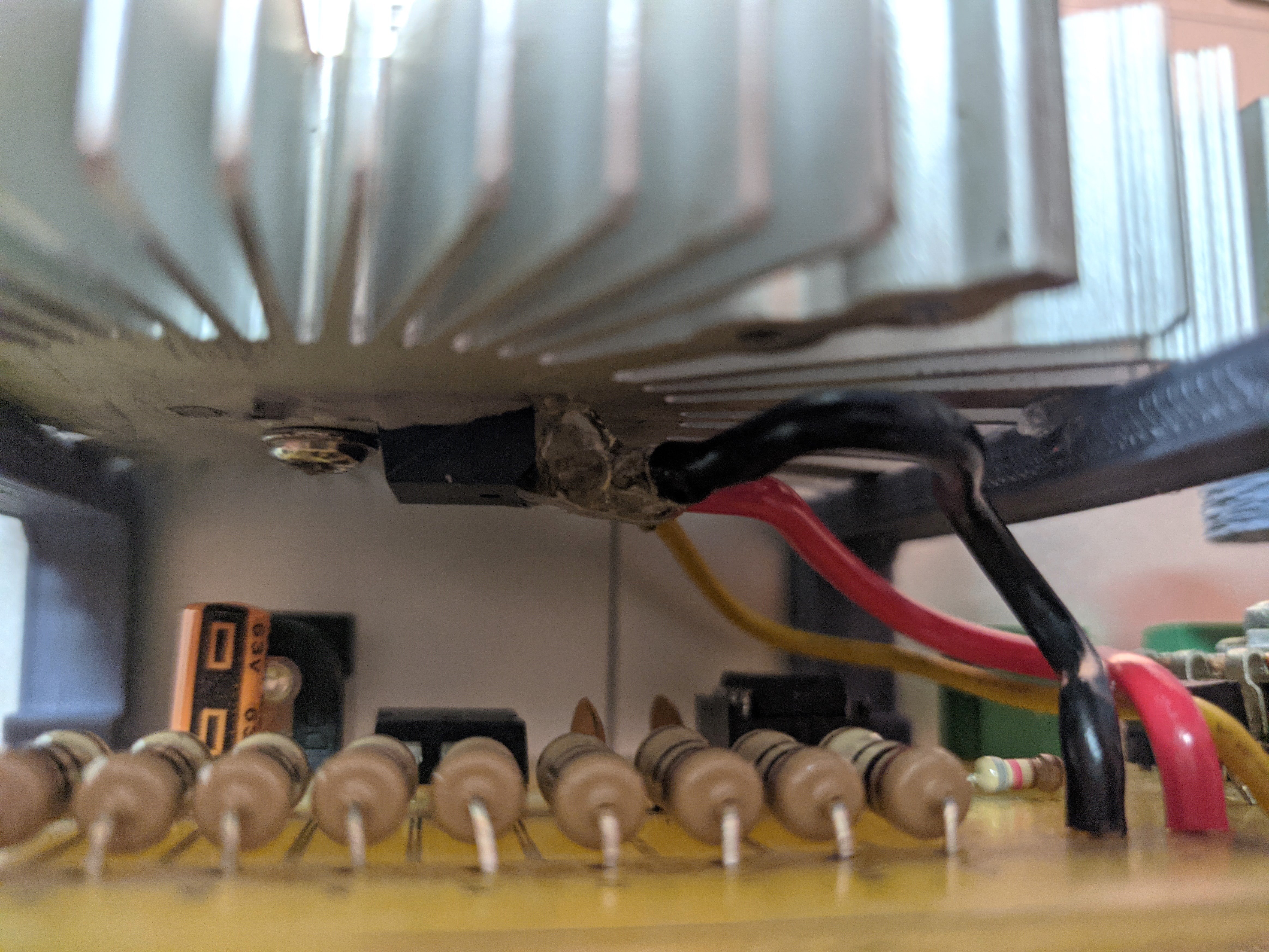
There is no built-in ammeter, just to save space and almost everyone has two or more multimeters. It's important to note that the device won't function without an ammeter connected across the current probs since it's needed to complete the circuit. Also, keep the load polarities as per the labels on the PCB, especially when using to test batteries. A separate voltage regulator ( 12v ) was added so as to maintain a stable supply voltage. Since it's a 12v regulator it's important to use a DC adaptor or supply voltage of a minimum of 14v since these linear regulators have a dropout voltage ( 2v for 78xx series regulators).
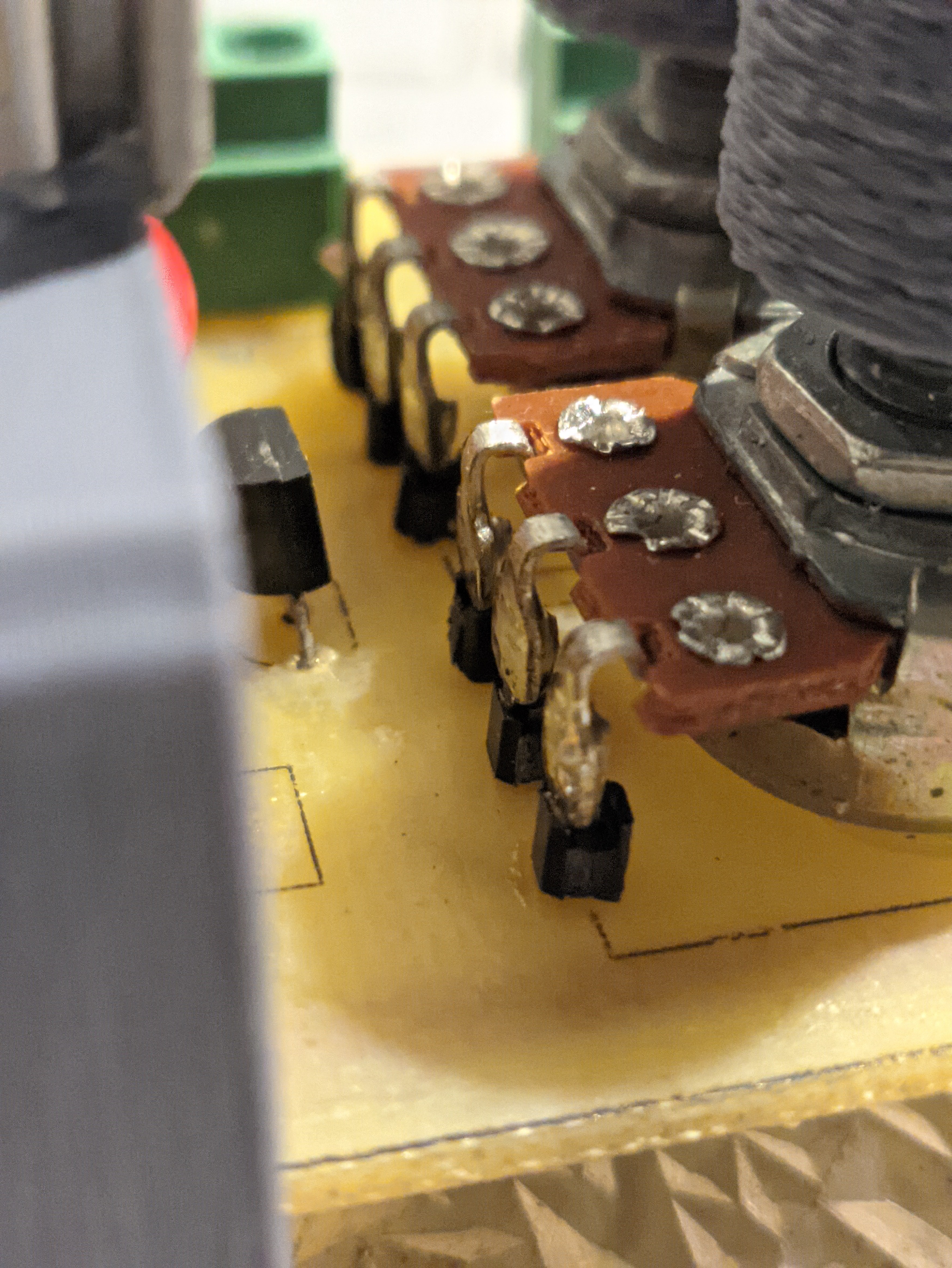
A set of resistors in parallel was chosen since it provides a better tolerance value and is also a better choice compared to having chunky ceramic cement or wire-wound resistors. Having resistors in parallel also has the advantage of increased power handling capability meaning a set of ten, 1-ohm resistors of 1 watt can handle a max power of 10 watts. With a max current rating of 2.5 A, resistors would have to dissipate 6.25 watts ( 2.5 x 2.5 x 1 ) under maximum load conditions, which is well within the limits. Also, a set of fine and coarse adjust potentiometers was added to allow for fine-tuning. The PCB design accommodates potentiometers of the ER-1612 vertical package, it's also possible to solder some male pin headers to the potentiometers to mount them on the PCB ( as shown in the image below). This can be easily replaced by a single multiturn potentiometer if that's what you want. In that case, connect the middle pin of the multiturn pot to pin 2 of RV2, one end to the ground and the other end to pin 1 of RV1.
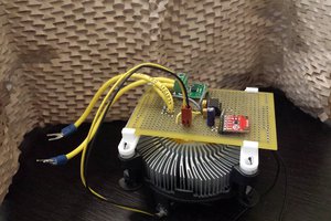
The PCB design was kept single-sided so as to make it easy for home fabrication. All the components are through-hole type and the footprint of the MOSFET is of a larger package ( TO-247 instead of TO-220 ) this was done just to allow for some clearance between wider traces. This doesn't matter much since the MOSFET is supposed to be mounted separately by using some wires instead of directly to the board. Some 3d printable heatsink holder designs have been uploaded, print two of the tall ones and a pair of short ones ( print these in PETG or ABS ). They are designed to be clipped onto the PCB, so it's important to stick to the dimensions of board edge cuts to allow for the best fit. Two small holders can be clipped onto the front ends, and some hot glue on the ridge can help it stay in place. They have extended legs below to act as standoffs.
There are no mounting holes designed onto the heatsink holders. This is mainly because not everyone has access to the same type of heatsink with standard holes. So I recommend using silicone sealant to stick the bottom of the heatsink to the holder after mounting the MOSFET onto the heatsink. Silicone sealant can easily go to temperatures of 200 C and can be disassembled without...
Read more »
 Bud Bennett
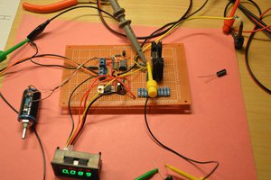
 w_k_fay
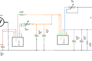
 MrWunderbar