Close
0%
0%

"High" Bandwidth - Current Sense Amplifier

Configurable gain and bandwidth current sense amplifier. DC to 1MHz/100kHz bandwidth, at 25x/50x gain.

Similar projects worth following
This is one of those projects that has stuck with me for several years. I tend to revisit this design as I learn new topics… and occasionally scratch my head on past design decisions. The main issue I ran into in the past was, although the device was functional, it wasn’t all that useable. More often than not, I’d characterize the CSA (current sense amplifier) then shift it to the bin of “completed” projects. This time around I hope to finish a polished design that I actually WANT to use in my home lab. To accomplish this, my new design is heavily focused on simplicity, low effort configurability (less trimmer pots), and uncalibrated out of the gate precision.

Current Project Status

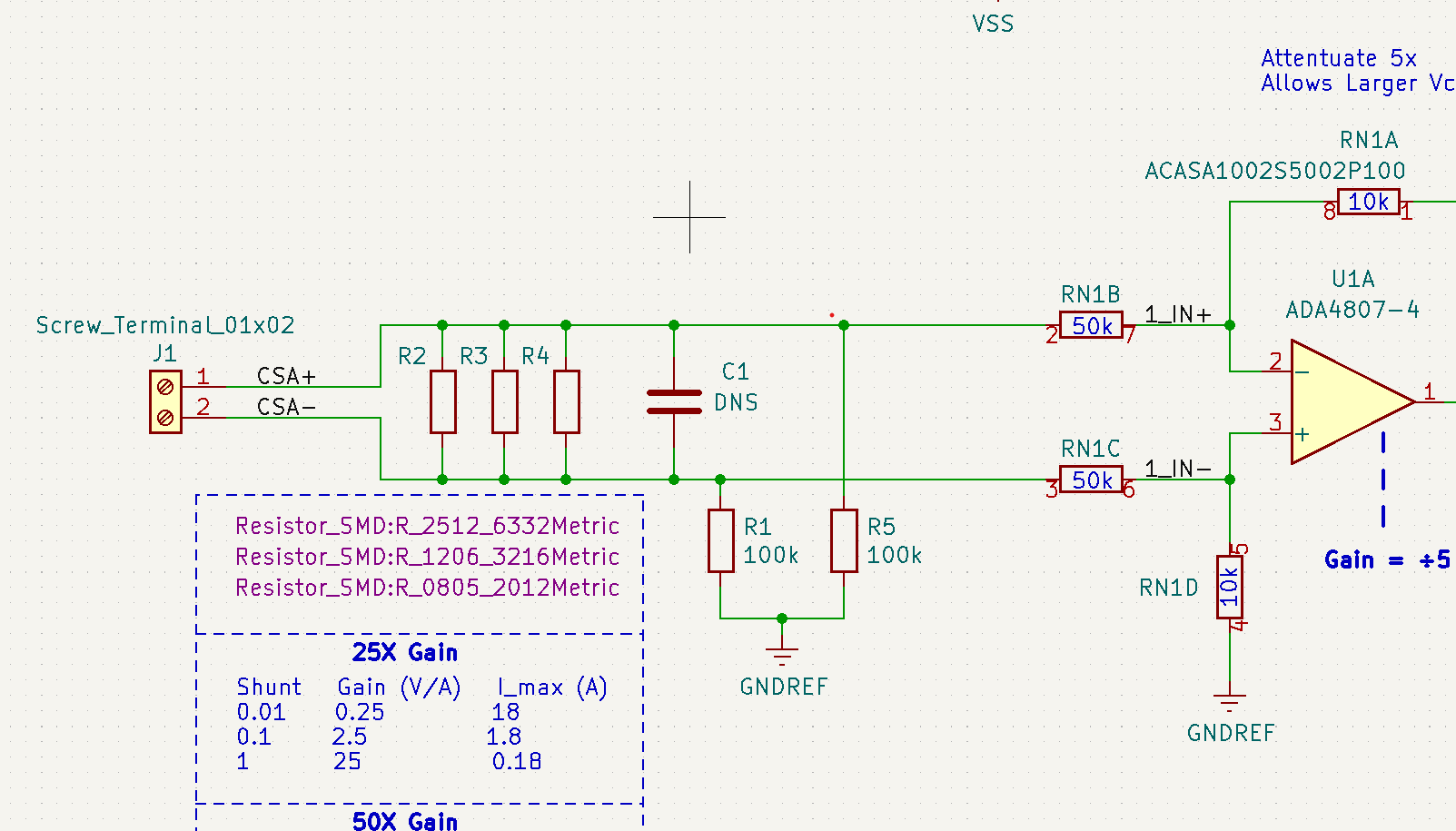
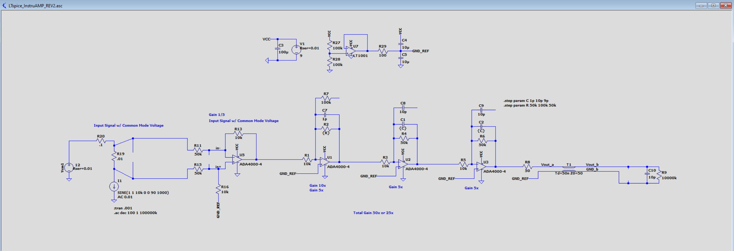
Schematic ------------------- ( ✓ )

PCB Layout ----------------- ( ✓ )

Documentation ------------ ( ✓ )

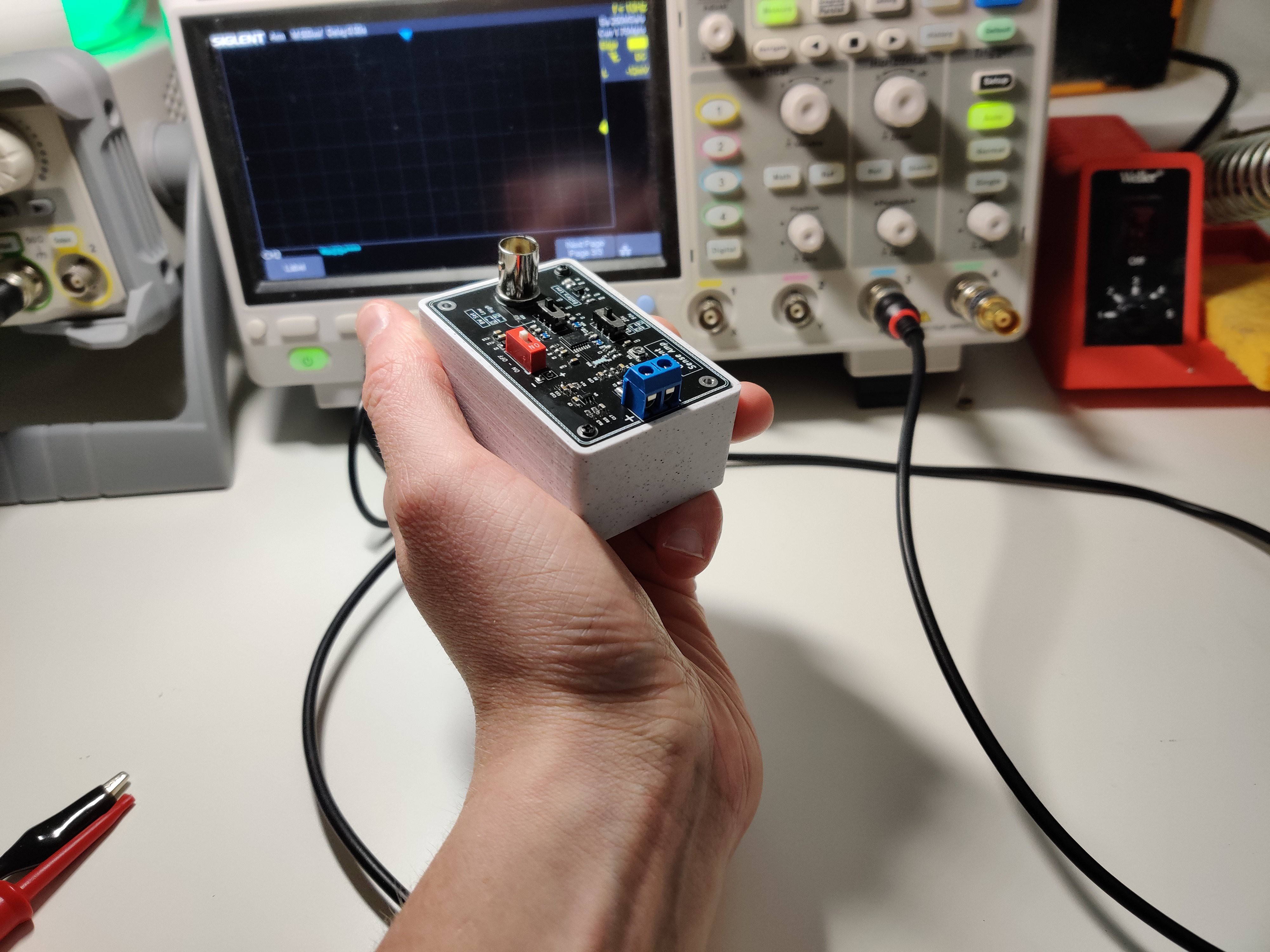
Order + Assemble -------- ( ✓ )

Push 2 Hackaday --------- ( ✓ )

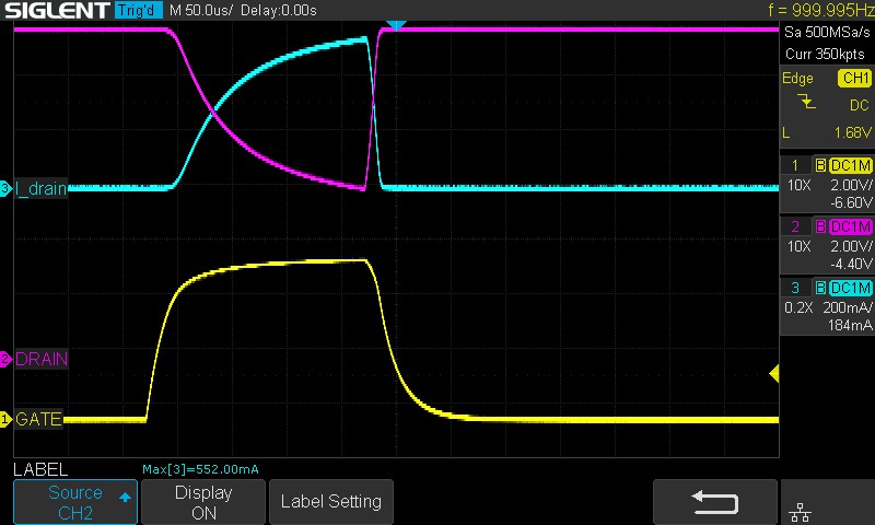
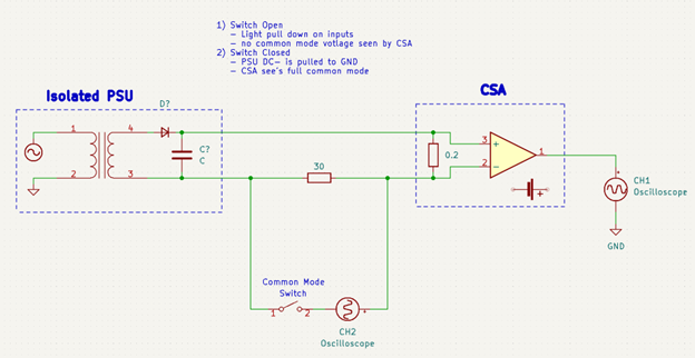
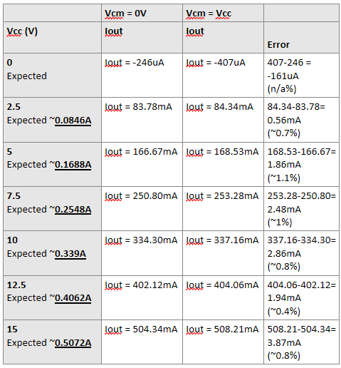
LAB: Common Mode ----- ( ✓ )

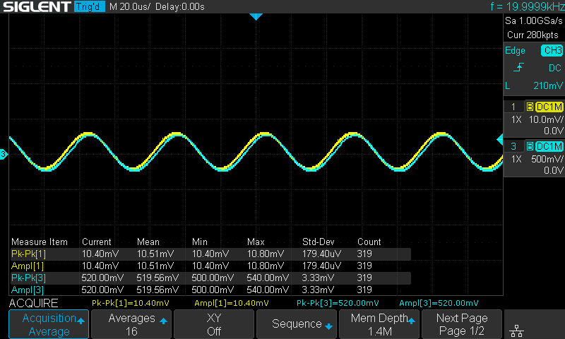
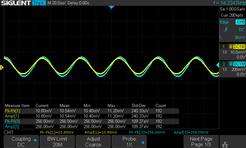
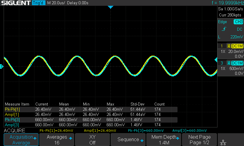
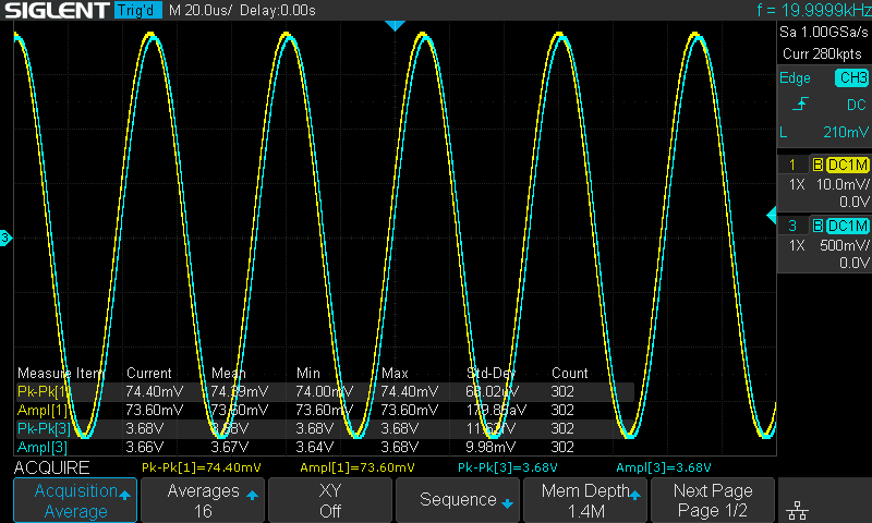
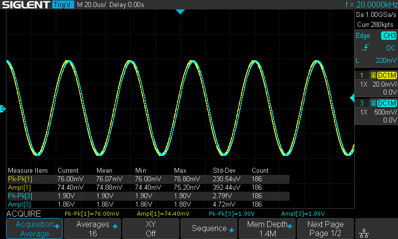
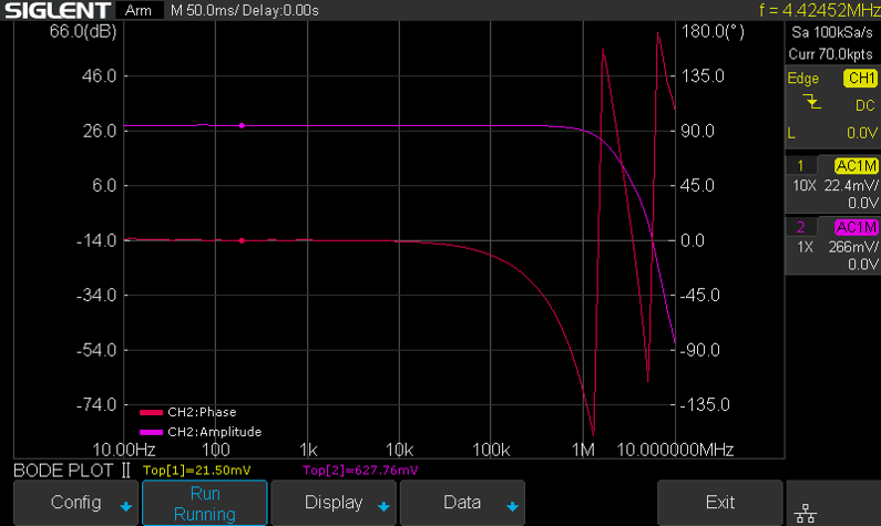
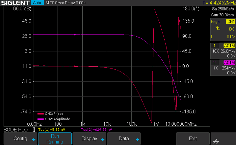
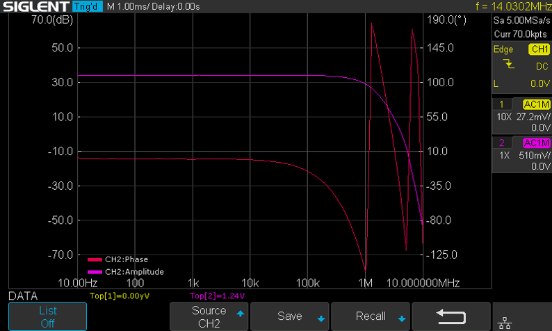
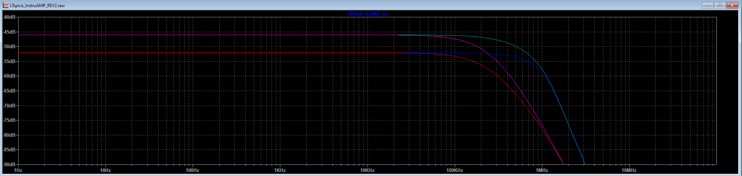
LAB: Bandwidth ------------ ( ✓ )

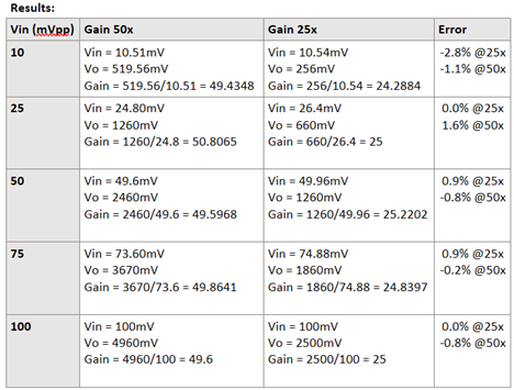
LAB: Accuracy -------------- ( ✓ )

Future Work --- Cleanup Documentation [ maybe :) ]

CsaBOX.step

Step file for the container. Could probably use some tweaking but it does what it needs to....

step - 64.58 kB - 06/18/2023 at 15:16

Download

ibom.zip

Interactive BOM from Kicad Plugin

x-zip-compressed - 134.55 kB - 06/18/2023 at 01:27

Download

Schematic.pdf

17.June.2023 Schematic

Adobe Portable Document Format - 139.84 kB - 06/18/2023 at 00:15

Preview
Download

x-zip-compressed - 131.77 kB - 06/04/2023 at 23:56

Download

  • 1 × https://www.digikey.ca/short/78j21jr0 Link contains 1x assembly components

  • Conclusion

    Jesse Farrell06/17/2023 at 23:41 0 comments

    Based on my testing I’ve designed about a 1-2% accurate CSA. Not the accuracy I was shooting for, but its good enough for a quick sanity check and general debugging. The widget is able to manage common mode voltages tested up to 15Vdc, and has a bandwidth of about 100-500kHz. Again, this is enough for most hobbyist circuits. I also designed a quick enclosure for the CSA in fusion 360 that will be pushed to the project files shortly.


    Future Recommendations…

    In my eyes, the disappointing spec for this design was the bandwidth. Due to component availability, I was forced to go with network resistors 10x higher impedance than what I wanted; (10k/50k) when I was hoping for (1k/5k). The higher impedance allows parasitic capacitance - for example at the inputs of the opamp - to more readily affect the overall bandwidth of the design. The MC33272A has 3pF typical input capacitance…. ☹

    (++ Reminder to future me, make the BNC connector R/A, and maybe switch to MMCX)

    CSA In Action….

    Here’s the thing in action. I’ve tossed together a low-side switch with an NMOS from my parts bin. CH1 is the gate voltage (Vgs) coming from my function generator, CH2 is the drain voltage (Vds), and CH3 is the current going through the drain (Idrain). Current goes through the CSA (0.2ohm) -> 10ohm Resistor -> NMOS Drain. 

    Why do I think this cool?

    How could we get a similar capture without the CSA…

    Use isolated scope – but these are pretty rare, and I personally don’t have one.

    Use a differential probe – but these cost a pretty penny (that's what the CSA fundamentally is)

    Use the scopes MATH – but this would take up 2 channels, and it slows down my scope

    Just accept 1 waveform – that’s no fun…

  • Testing – Gain Accuracy

    Jesse Farrell06/11/2023 at 22:00 0 comments

    In my previous post I found that the DC common mode rejection adds less than a percent or so of error to the output. Next, I’ll see how the overall gain accuracy looks. I’m using a 20kHz input signal, and testing the output at 50x and 25x gain configs.

    Measurements were collected at the input and output of the CSA. I had some averaging setup to help cleanup both waveforms. At lower input voltages the accuracy starts degrading, but above 25mVpp, the CSA gain is consistently within ±1% of expected. See data below.

    And because I have them, I might as well share some of the captures too.

    Vin (mVpp)

    Gain 50x

    Gain 25x

    10

    Expected ~

    Vin = 10.51mV

    Vo = 519.56mV

    Gain = 519.56/10.51 = 49.4348

    Vin = 10.54mV

    Vo = 256mV

    Gain = 256/10.54 = 24.2884

    25

    Expected ~

    Vin = 24.80mV

    Vo = 1260mV

    Gain = 1260/24.8 = 50.8065

    Vin = 26.4mV

    Vo = 660mV

    Gain = 660/26.4 = 25

    50

    Expected ~

    Vin = 49.6mV

    Vo = 2460mV

    Gain = 2460/49.6 = 49.5968

    Vin = 49.96mV

    Vo = 1260mV

    Gain = 1260/49.96 = 25.2202

    75

    Expected ~

    Vin = 73.60mV

    Vo = 3670mV

    Gain = 3670/73.6 = 49.8641

    Vin = 74.88mV

    Vo = 1860mV

    Gain = 1860/74.88 = 24.8397

    100

    Vin = 100mV

    Vo = 4960mV

    Gain = 4960/100 = 49.6

    Vin = 100mV

    Vo = 2500mV

    Gain = 2500/100 = 25

  • Testing – DC Common Mode Rejection (Test #2)

    Jesse Farrell06/10/2023 at 21:35 0 comments

    As mentioned in my earlier log, the last rejection test was a bit flawed. Here’s my second attempt. Unlike before there won’t be any AC signal injected on top the common mode, just a DC offset. This offset is supplied by an isolated lab bench PSU. See my test setup below.

    In this circuit the “Common Mode Switch” is what enables the common mode voltage. While this switch is open, a light pull-down in the CSA should essentially remove all common mode voltage. When the switch is closed (which I will do by clipping CH2 GND to DC-), the CSA will see the full common mode voltage riding on top of the 30ohm resistor. Here’s my actual setup….

    None of my tools are particularly precise/accuracy so it’s somewhat the blind leading the blind when it comes to these results. Nevertheless, these results are valuable in a comparison to one another... Note that I calculated the expected current using the CH2 mean divided by the measured resistance of the 30 ohm load (29.2ohm).

    Ok so the error added by common mode voltage is less than ~1%, at approximately 286uA/Vcm. I’d call that a success. 

  • Testing – DC Common Mode Rejection

    Jesse Farrell06/06/2023 at 04:05 0 comments

    A key aspect of this design was that it needed to reject atleast a 12V common mode signal. To achieve this, I attenuate both the common mode and differential signal at the first stage of my CSA (any other ideas??? I’d be interested to hear about them). This brought signal+Vcm to within the operating limits of my op-amp, but also substantially affects my S/N ☹. Anyhow, lets see how it turned out in practice with a few test points.

    Note that I’m only looking at DC common mode here since this is what I’ll typically encounter. I’ll likely do a sweep of the AC rejection later.

    Test signal is 50kHz, 50mVpp, AC coupled across the inputs of the CSA. The common mode voltage is provided by an external bench supply.

    Vcm=0V, Vo_mean = -0.3mV

    Vcm=5V, Vo_mean = 71.6mV

    Vcm=10V, Vo_mean = 132.55mV

    Well that was a bit disappointing, but I think my test setup is flawed. I added some series impedance to isolate my Vcm source, but this would have created a voltage divider at the R1 and R5 in my schematic. I’ll likely be doing some tweaking of both my circuit and test setup. (pretty sure I can DNP both R1 and R5 in this REV of my CSA)

  • Testing - Frequency Response

    Jesse Farrell06/05/2023 at 01:00 0 comments

    After some initial spark-up (pretty uneventful, magic smoke did not escape) I wanted to quickly take a look at the bandwidth. The following results were taken using OPA1664AIPWR as the main op-amp. Note that the spikie phase response is just the foldback from -180 to +180.

    25x @High BWL

    25x @Low BWL

    50x @High BWL


    50x @Low BWL

  • Simulation

    Jesse Farrell06/04/2023 at 20:28 0 comments

    Compulsory LTspice simulation. Note that I’m not too concerned which op-amps are used in the sim… this is just to validate the overall design. 

    As expected, our simulated bandwidth is a lower than the -3dB point calculated using 1/(2*pi*R*C). This is mainly caused by the cascading of amplifiers. To adjust this, we would need to tweak the feedback capacitors… but since we are using relatively high gain-set resistors, this isn’t too easy. Ideally, I’d be using lower resistances, but these aren’t in stock. (Wanted to use low drift, high spec ACAS network resistors… can use 0402 parts in place though).

  • General Background

    Jesse Farrell06/04/2023 at 19:40 0 comments

    Single chip CSA solutions exist, but all fall short in one aspect or another. Whether it be the low bandwidth of the INA27x series, limited configurability of hall-effect options, or just part availability.

    The main goal of this design is to provide a simple circuit that will work with a wide range of IC’s on the market, and can be used (or adapted) for many different applications. To accomplish this, I first found what was the most common 4-channel op-amp package. Turns out 14-TSSOP (0.173", 4.40mm Width) is one of the most common packages for in stock op-amps. To support lower spec’d devices I included some options to compensate the total offset voltage, and to compensate the offset voltage caused by op-amp bias current.

    For more information see the HAB document… I’ll be keeping these logs somewhat brief, and more testing focused.

View all 7 project logs

  • 1
    Quick Start

    1.) Order Boards

    • Gerber files provided at Gerbers(June.4.2024).zip in project files 
    • Personally used JLC for board FAB

    2.) Order parts

    • Here's a Digikey cart full of all the parts for 1x board https://www.digikey.ca/short/78j21jr0
    • Consider using a different shunt resistor (labeled R3 in the digikey Cart)
      • Output swing is primarily limited by the supply rails... depending on the shunt resistance we'll hit the rails faster
      • Max input current = (Vcc_min/2)/(50 * Rshunt) = (4.5V/2)/(50*Rshunt) = 0.045/Rshunt [A]

    3.) Solder the board

    • See IBOM in project files

    4.) Clean the board and LET IT DRY

    • Any residue left on the board DOES lead to "fun" analog goodness

    5.) Connect a 9V battery and start measuring... use the following process

    • a) PWR the device
    • b) Set the CSA gain + bandwidth
    • c) Correct the DC offset
    • d) MEASURE

View all instructions

Enjoy this project?

Share

Discussions

Similar Projects

Does this project spark your interest?

Become a member to follow this project and never miss any updates