Close
0%
0%

Bootstrapping a ROMless Z80 using RS-232

Is it possible to bootstrap a simple ROMless Z80 system using only two wires - e.g. from an RS232 interface? This project explores this.

Similar projects worth following
If you have a Z80 CPU, RAM chip, clock signal, and some resistors, is it possible to bootstrap via an RS232 interface (using the Transmitted Data and Request to Send signals)?

It could perhaps be done like this:

During bootstrapping, ensure that RAM cannot output to the bus by using a manual switch that disconnects RAM /OE from Z80 /RD, and pull RAM /OE high.

Use resistors to connect Z80 data lines to address lines in such a way that as the Z80 increments through addresses, the pattern of bits appearing on the data pins is an instruction sequence that causes writes to RAM. If the clock generator uses 2 gates from a 7400 quad 2-input NAND gate then it would be possible to use this to make two of the data lines a NAND of some of the address lines. Ensure that one of the instructions thus executed is the HALT instruction. One of the RS232 signals (probably the Transmitted Data signal) is used to resume execution after HALT. The other is used to influence the data written to RAM.

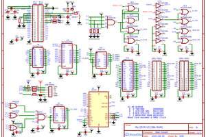
The main motivation for this project is that as a hobbyist I want to make a simple Z80 system without having to bother with programming non-volatile memory. Devising a ROMless bootstrap scheme enables this, and also reduces the amount of wiring involved. Another way of looking at it is that the boot ROM is so simple that it can be implemented with a handful of diodes and resistors rather than an IC.

This scheme could also be useful in systems that include a Z80 alongside another processor - the other processor could provide a four-wire output that could be used to bootstrap the Z80, removing the need to have a ROM for the Z80.

It could also be used as an in-circuit programming method to program the flash memory in a Z80 system that has RAM and flash memory. This would require a switch that makes RAM map to the whole address space during bootstrapping, the lower part during flash programming, and the upper part during normal operation.

  • Z80 on solderless breadboard

    will.stevens02/03/2024 at 08:52 0 comments

    I’m making the circuit for this project using things I have in my parts box - a lot of the parts are salvaged from computer systems dating back to the 1980s and 1990s. The Z80 is a Mostek part manufactured in 1983 and last used in 1995. I made a 4MHz clock circuit using a 74LS04 as per the series resonant schematic on this page.

    I pulled all Z80 inputs to 5V using 47k resistors, and pulled the data bus to 0V so that the Z80 executes NOP instructions.

    I’m using a Velleman HPS140i to check that the Z80 appears to be operating. Connecting the scope probe to address bit A11 shows the expected 1KHz square wave.

  • Program for driving the boot process

    will.stevens02/03/2024 at 07:11 0 comments

    I’ve added a link to the GitHub repo ‘TwoWireBootZ80’ which will be used for the program that will run on a PC to drive the booting process. The program is written in C because I already have some code for using the serial port written in C, and I’ll be compiling and running it on an ancient laptop  (an Asus Eee PC) that I use for electronics projects.

    The core of the program is this function:

    void SetMem(unsigned char *m, int n)
    {
      unsigned char l=0;
    
      for(int i=0; i<n; i++)
      {
        m[i]=(m[i]+0xDC) & 0xFF;
    
        if (m[i] > l)
          l = m[i];
    
        SetAtHLIncHL();
      }
    
      for(;l>0;l--)
      {
        printf("Iteration l=%d\n",(int)l);
        for(int i=0; i<n; i++)
        {
          if (m[i]<l)
            SetAtHLIncHL();
          else
            IncAtHLIncHL();
        }
      }
    }

    It works by first of all sweeping through RAM and initialising every byte to 24h.

    Then on successive sweeps it keeps some bytes fixed at 24h, and allows others to increment. For example, any bytes that need to be set to 25h would be allowed to increment only on the last sweep through RAM. Any byte set to 26h increments on the last two sweeps and so on. There could be upto 255 sweeps, if any bytes need to be set to 23h.

    The program hasn’t been tried yet, so it may not work correctly.

  • Setting HL to a defined value

    will.stevens02/01/2024 at 07:26 0 comments

    Since HL is undefined on power on, it is necessary to fill RAM with a sequence of instructions that will set it to a known value, regardless of where in that sequence of instructions execution begins.

    One way is to fill RAM with 21h, so that LD HL,2121h gets executed again and again.

    Another way is to fill RAM with DEC HL, with a single HALT somewhere in RAM being the last byte written using the bootstrapping scheme. HL points to the address following HALT. When execution starts HL will be decremented until HALT is reached. This means that whereever the HALT instruction is in RAM, HL will have the value 0001h by the time HALT is executed. I prefer this to the LD HL,2121h idea, because the Z80 has a pin indicating the HALT state, which will give some indication that bootstrapping is working correctly.

  • Further refinement

    will.stevens01/22/2024 at 07:26 0 comments

    The following two instruction sequences differ by only a single bit in the first instruction:

    00110110 LD (HL),n
    00100011 23h
    01110110 HALT
    
    00110100 INC (HL)
    00100011 INC HL
    01110110 HALT

    Each bit except D1 is either 0,1,A0,A1,/A0

    D1 = A0 or A1 or RTS


    By executing sequence 1 and sequence 2 alternately, the whole of memory can be filled with a constant value (24h)

    By executing sequence 2 alone over and over again, the whole of memory can be incremented by one.

    By mixing sequence 1 and sequence 2 we can keep some locations fixed at 24h and increment others.

    A procedure to fill RAM with any desired contents (but offset by an unknown address) is to start by alternating sequence 1 and sequence 2 then on each sweep through memory we can omit some sequence 1s to ‘release’ bytes which had been held at 24h, so that they start incrementing.

    The issue of unknown offset can be resolved by first filling RAM with a single LD HL,nn and setting all other bytes to a harmless opcode. Then execute the contents of RAM. Then run the procedure again, this time with a known offset.

  • Another approach

    will.stevens01/21/2024 at 09:05 0 comments

    Here is another approach that is based on using HL to point to locations in RAM, and then using opcodes that increment or set the location that HL points to. This approach doesn’t need a separate ‘initialisation’ step, but can only write 256 bytes to RAM. The page to which these bytes get written is undefined - that doesn’t matter because we first fill all of RAM with ‘harmless’ LD H,E opcodes and these get executed until the PC reaches the 256 byte page.

    The data bits are set as follows, we need an inverter for A0, one NAND gate and one OR gate.

    D7=0
    D6=A1
    D5=1
    D4=A0
    D3=0
    D2=/A0 nand RTS
    D1=A1 or RTS
    D0=/A0

    This gives the following instruction sequences when RTS=1 and 0 respectively

    00100011 INC HL
    00110110 LD (HL),n
    01100011 63h
    01110110 HALT
    
    00100101 DEC H
    00110100 INC (HL)
    01100111 LD H,A
    01110110 HALT

    First we execute the first (RTS=1) sequence to fill RAM with 63h (LD H,E). Then we execute the second sequence (RTS=0) enough times  to set one byte in RAM (we don’t know which) to 2Eh (LD L,n). When we run the contents of RAM this has the effect of setting L to a known value. We can then use the two sequences above to increment HL until L=0, and then fill 256 bytes with any desired contents. The details of the method for doing this will be described in a future edit to this log entry.

  • More simplification

    will.stevens01/16/2024 at 21:42 0 comments

    Here is a simpler scheme. Rather than connecting RS-232 TxD to /NMI, it is connected to /RESET, and this is used to reset the CPU whenever HALT is reached. This scheme assumes that all registers except PC (and I and R) are preserved on RESET.

    The following instruction sequence is used for programming memory:

    23 00100011 INC HL
    E5 11100101 PUSH HL
    76 01110110 HALT
    F6 11110110 OR A,n

    This can be obtained using the following assignments:

    D7 = A0
    D6 = A0 or A1
    D5 = 1
    D4 = A1
    D3 = RTS and /A1
    D2 = A0 or A1
    D1 = A1 or /A0
    D0 = /A1

    To initialise HL, set D1 = A1 (with a manual SPST switch). This makes the first instruction LD HL,nn followed by OR A,n (which causes LD HL,nn to be skipped on the second time through the sequence), then PUSH HL, then HALT.  So HL gets set to the value 76E5h.

    The sequence can be used to push any desired sequence of bytes onto the stack by selectively omitting the PUSH while counting to the required value of HL. This is done by setting RTS high, so that the sequence becomes DEC HL, EX DE,HL, HALT. Because of the EX DE,HL instruction this must be executed twice to decrement HL once. So HL can be set to any required value and then pushed onto the stack by setting RTS low again. 


    Because we don’t know the value of SP when we power on, the first thing we do is use the above scheme to fill RAM with the LD SP,HL instruction. Then we execute this so that SP has a known value.


    We then run the programming scheme again starting with the stack at a known location, so that we can fill RAM with whatever we like.


    Filling RAM with a constant value can be quick (2 bytes every third time /RESET is set low) - 1Kb in about a 0.15 seconds at 115200 baud. (Assuming each dummy byte sent to TxD causes one reset).


    Filling RAM with a program
     would be slower, since on average we must decrement HL by about 32768 before every PUSH HL. That is about 15 million decrements per 1Kb RAM. That is 30 million resets and would take about 3000 seconds at 115200 baud.

    The speed can be improved by doing more than one reset per TxD dummy byte - up to 5 can probably be done by transmitting “start bit + 01010101” so 600 seconds to program 1Kb of RAM.

    But if we only need to load a short program to do the next stage of bootstrapping, this might only be 100 bytes long, and would only take a minute.
     

  • Simplification

    will.stevens01/14/2024 at 09:02 0 comments

    I’ve been thinking more about initialization, and I think that it is sufficient to initialise A, and leave initialization of everything else to the first boot program written to RAM. Then write a second boot program (i.e. any 256-byte program) after that. The rationale is that:

    • It doesn’t matter which 256-byte block of RAM the first boot program is written to, because the rest of RAM is filled with harmless instructions.
    • Initialization of H,L and SP can be done with 3 single-byte instructions (assuming A is already initialised). So a repeating pattern of those 3 instructions + HALT can be the first boot program. 
    • Because the 4 instructions are repeated again and again, it doesn’t matter where in the 256 byte block they are (so the initial value of L doesn’t matter) and it doesn’t matter what gets overwritten by the stack, so long as at least one instance of each instruction is executed. 

    The sequence to initialise A is:

    3E 00111110 LD A,n
    2E 00101110
    76 01110110 HALT
    76 01110110 HALT

    This sequence only needs to be executed once.

    The programming sequence is:

    3D 00111101 DEC A
    2C 00101100 INC L
    77 01110111 LD (HL),A
    76 01110110 HALT
    
    followed by this after NMI
    (PC=0066h)
    
    F7 11110111 RST 30h


    The sequences only differ in how D1 and D0 are configured.

    For the programming sequence the configuration is:

    D7=A2
    D6=A1
    D5=1
    D4=A1 or /A0
    D3=/A1
    D2=1
    D1=A1
    D0=/A0

    For the initialisation sequence it is as above except D1=1, D0=0. So a DPDT can be used to switch between the two.

    So the complete sequence of steps required to bootstrap the system will be:

    • Disable /OE on RAM with a manual switch
    • Ensure DPDT switch is set to ‘initialise’
    • Start running host program on PC that sets up serial port (using fastest available baud rate) and sets RTS signal coming into the Z80 system to zero.
    • Power on the Z80 system
    • Wait for a second
    • Switch the DPDT to ‘memory program’
    • Tell the host program to program the first boot program.
    • When programming has finished, reenable /OE.
    • Tell the host program to send several NMIs to ensure that the 4 byte sequence of the first boot program is executed at least once.
    • Disable /OE again
    • Switch the DPDT to ‘memory program’
    • Tell the host program to program the second boot program (i.e any 256 byte program)
    • When programming has finished, reenable /OE.
    • Tell the host program to send an NMI to start executing the second boot program.

  • Additional thoughts about initialization

    will.stevens01/13/2024 at 15:42 0 comments

    Looking at the Z80 opcode table, another way to initialise HL and AF (but not SP) is to connect the data lines up as follows:

    D7 = 0
    D6 = A4
    D5 = A3
    D4 = A2
    D3 = A1
    D2 = 1
    D1 = 1
    D0 = 0

     This has the effect of executing:

    LD B,06h
    LD C,0Eh
    LD D,16h
    LD E,1Eh
    LD H,26h
    LD L,2Eh
    LD (HL),36h
    LD A,3Eh
    LD B,(HL)
    LD C,(HL)
    LD D,(HL)
    LD E,(HL)
    LD H,(HL)
    LD L,(HL)
    HALT

    Leaving SP uninitialised is not necessarily a problem. Although the “memory program” sequence writes to stack, that could be avoided by switching from using NMI to restart execution after HALT to using RESET to do this.

    But the stack writes in the “memory program” step do serve a purpose - they are for initialising the whole of memory with harmless instructions, which will execute until the 256-byte block of ‘programmed’ memory is encountered. This memory initialisation is done before the 256-byte block is programmed. If we don’t know where SP is initially, we won’t know whether it accidentally overwrites the 256 block we are programming. But switching TxD from NMI to RESET after all of RAM has been initialised by stack writes will prevent any further stack writes, so the 256-byte block won’t be overwritten.

  • Corrected initialisation sequence

    will.stevens01/13/2024 at 07:01 0 comments

    The previous log entry incorrectly stated that SP is initialised to 0000 on reset. This isn’t true - it is undefined - so it needs to be initialised too. Here is a sequence that will do this:

    E1 11100001 POP HL
    F1 11110001 POP AF
    31 00110001 LD SP,nn
    31 00110001 
    E3 11100110 
    F6 11110110 OR n
    76 01110110 
    76 01110110 HALT

    Because LD SP,nn is executed after POP HL and POP AF, this code needs to be executed twice, which can be achieved by pressing reset a short time after power on. You can see above that the data bits are still a fairly simple function of the address bits. A 6PDT switch will be needed to switch between this sequence and the “memory program” sequence described in the first log entry.

    So the complete sequence of steps required to bootstrap the system will be:

    • Disable /OE on RAM with a manual switch
    • Ensure 6PDT switch is set to ‘initialise’
    • Start running host program on PC that sets up serial port (using fastest available baud rate) and sets RTS signal coming into the Z80 system to zero.
    • Power on the Z80 system
    • Wait for a second
    • Press RESET 
    • Wait for a second
    • Switch the 6PDT to ‘memory program’
    • Tell the host program to run programming mode.
    • When programming has finished, reenable /OE.
    • Tell the host program to send a final NMI to start the Z80 executing from RAM.

  • Suppressing INC L and initialising HL and A

    will.stevens01/11/2024 at 07:16 0 comments

    Suppressing the INC L instruction can be accomplished by setting D5 = D4 or RTS.

    Initialising HL and A can be done using POP HL and POP AF, since the result of the ‘dummy’ memory reads performed during execution of these depend only on the value of SP (which is initialised to 0000h at reset).

    The following sequence will do it (I’ve put the hex and binary code for each instruction next to the instruction). The 3rd instruction in this sequence was chosen to make the data lines a simple function of the address lines. Because HL is initialised before LD H,(HL) is executed, it will set H to a function of HL - i.e. a constant value.

    E1 11100001 POP HL
    F1 11110001 POP AF
    66 01100110 LD H,(HL)
    76 01110110 HALT

     You can see that each bit here is either constant or equal to A0 or A1 or their negation:

    D7=/A1

    D6=1

    D5=1

    D4=A0

    D3=0

    D2=A1

    D1=A1

    D0=/A1


    So we can initialise A and HL by using this setup first, then manually switching to the setup described in the previous log entry after the HALT instruction is executed but before the first NMI. I think that this switchover can be done using a single 4PDT switch.

    Since the ‘or’s appearing in the data line expressions in the previous log entry can be implemented using diodes, I think that this bootstrapping scheme can be made without any additional ICs, so this ROMless bootstrapping scheme will use only 3 ICs in total: A 7400 quad 2-input NAND gate which is used to generate the clock signal and to invert A0 and A1. A static memory chip (I’m going to use an old 6116 2Kx8 RAM because I have a lot of old ones in my parts drawers), and the Z80 itself.

    I will draw a schematic when time permits, and also try to describe the scheme in more detail, because I don’t think I’ve clearly expressed the idea.

    It’s possible that I’ve made some mistake in thinking about this, but hopefully any mistakes will come to light in the course of writing it down in more detail.

View all 11 project logs

Enjoy this project?

Share

Discussions

Matthias Koch wrote 01/21/2024 at 13:29 point

A long time ago, bootloading of a Z80 using clock, reset and nmi was developed: http://www.z80.info/jmz8boot.htm

I think you can get inspiration from that!

  Are you sure? yes | no

will.stevens wrote 01/21/2024 at 17:03 point

Thanks, that’s an interesting link.

  Are you sure? yes | no

Ken Yap wrote 01/13/2024 at 09:24 point

Thanks, interested to see how this goes. 👍🍿

  Are you sure? yes | no

Similar Projects

Does this project spark your interest?

Become a member to follow this project and never miss any updates