This circuit is purely analog. The only active components are a LM324 quad op-amp and STP40NF10L N-channel MOSFET. D2 is a 10V Zener diode (1N4740A), R7 is a 20mOhm shunt resistor, and R9 is a trimpot that sets the minimum charge current. Other than that, it's just parts bin resistors and caps.
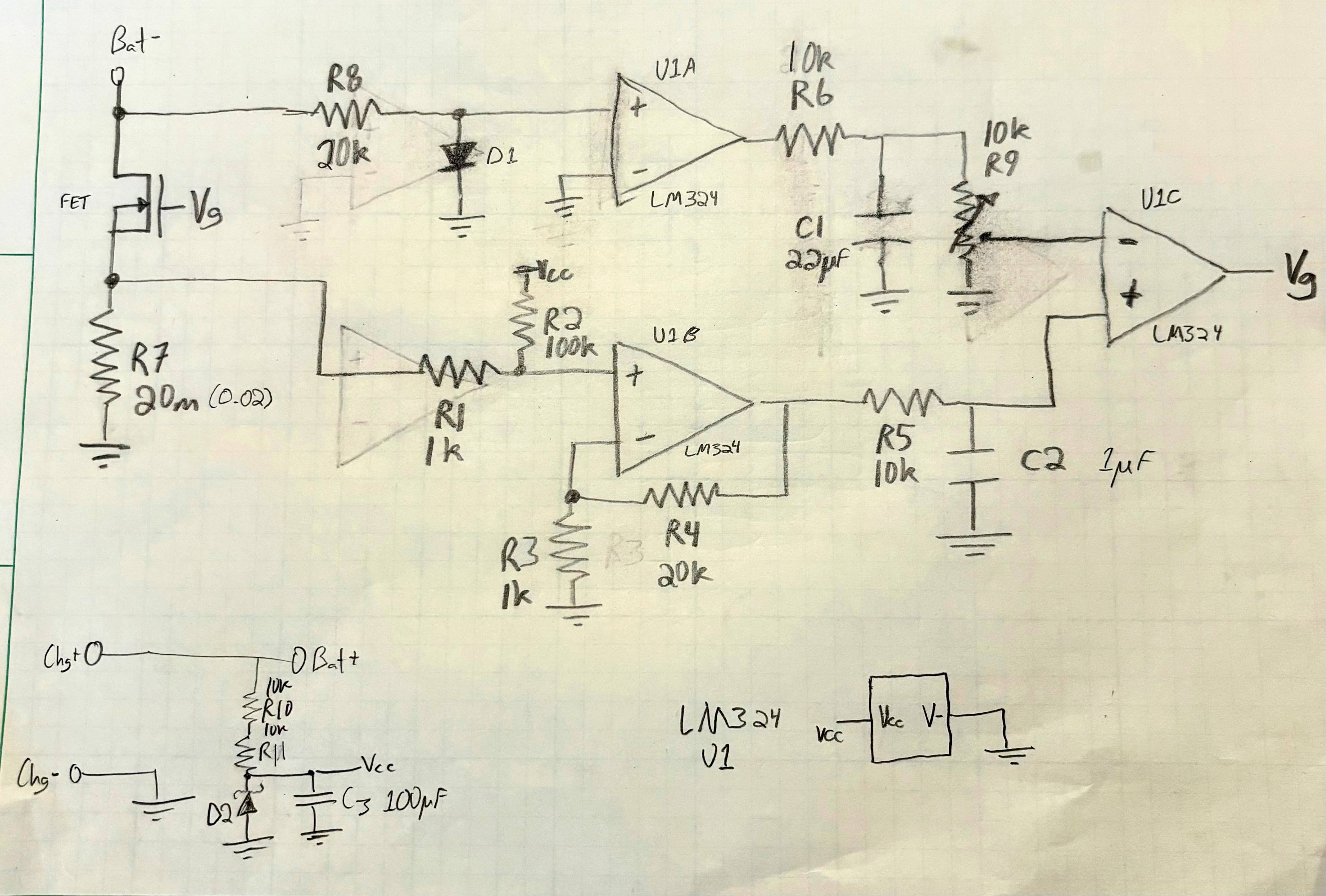
Here's how it works:
- We'll start off in the idle state. The circuit is connected to the battery, but the charger isn't connected. There's around +60V between Bat+ and Bat-, so Vcc is held at 10V by D2, a 10V zener diode. The supply current from the circuit flows from ground through the FET body diode to Bat-, so ground is actually at a positive voltage relative to Bat-. Bat- pulls the + input of U1A below the - input, so the output of U1A is driven low.
- U1B is our current sense amplifier. In the idle state, the voltage of our shunt resistor R7 is pretty much 0 so the voltage of U1B+ is just set by the voltage divider formed by R2 and R1. The output of this divider is (1k/101k) * Vcc which is about 0.1V. The output of U1B is this voltage multiplied by the gain, which is set by R4 and R3, so it's (1+20/1) = 21x. This provides a voltage of about 2.1V to the + input of U1C.
- U1C acts as a comparator and drives the FET that controls the charge current. Since U1A is providing 0V to its - input and U1B is providing 2.1V to its + input, U1C drives its output to Vcc, which turns on the FET, allowing charge current to flow.
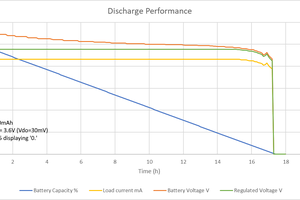
- When a charger is connected and starts supplying current, Bat- rises to a positive voltage relative to ground. This causes U1B to pull its output high, which starts charging C1 through R6. Over the next few hundred milliseconds, our minimum charge current threshold rises as C1 charges until it reaches its steady-state voltage.
- Meanwhile, the output of U1B, our current amplifier, is increased by the voltage across our shunt resistor R7. As long as the output of the current amplifier (U1C+) stays above the threshold voltage set by C1 and R9, Vg will be kept at Vcc and charge current shall pass.
- Once the charger hits the CV phase, charge current should start to drop. This, in turn, decreases the voltage across R7 which decreases the output voltage of U1B. At some point, U1B's output will drop below our threshold voltage at U1C's - input and the U1C's output will drop, shutting off our FET and terminating the battery charging.
- The circuit gets reset when the charger is disconnected from Chg- and Chg+. This causes Bat- to fall below ground, which drives the output of U1A to ground, which discharges C1, which brings our current threshold back to zero and turns on the FET again.
All in all, there's probably a way to do all this with a 555 timer but I had an LM324 lying around.
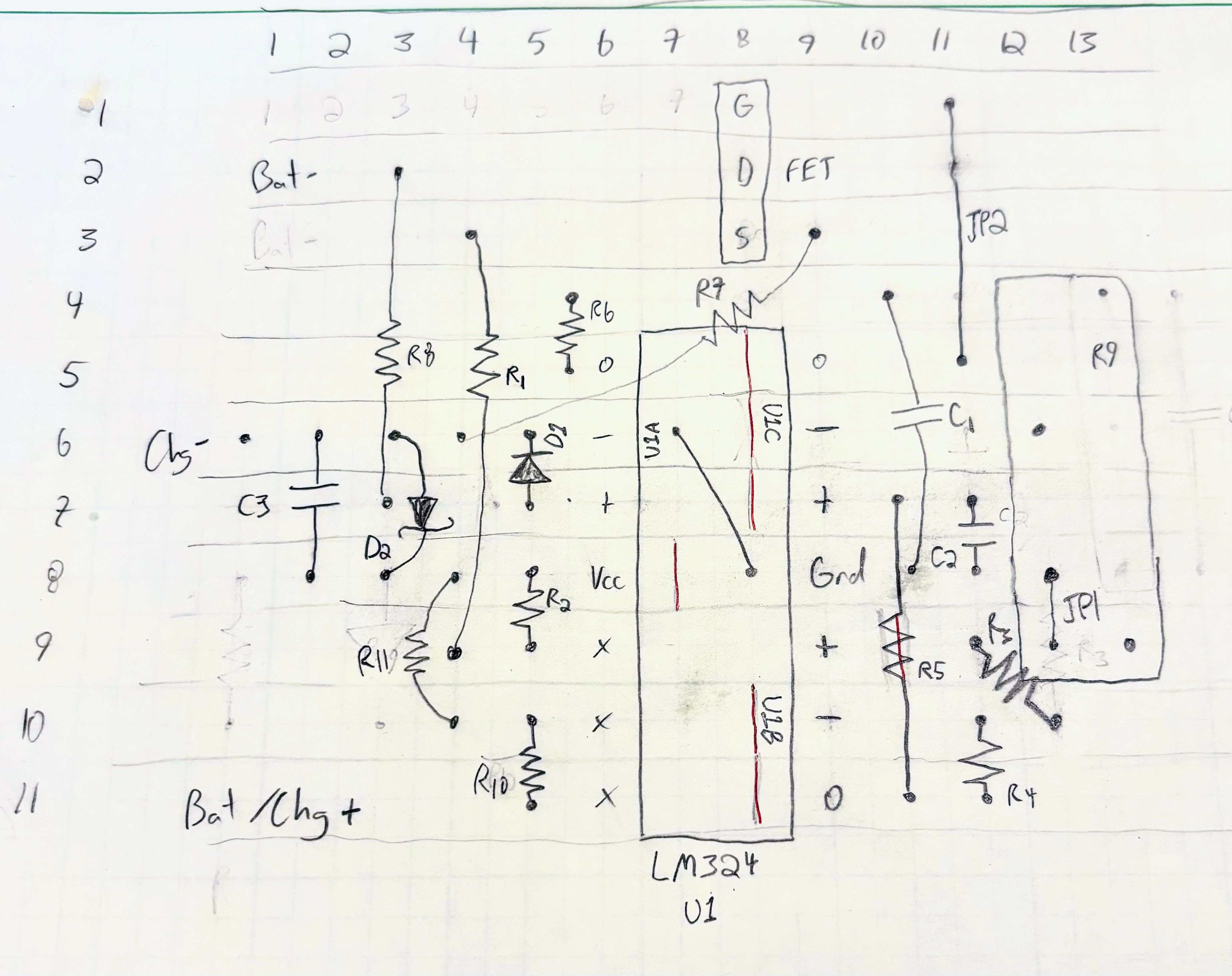
After plenty of breadboarding, I put together the circuit on a 0.1" spaced protoboard that had traces along the rows. Here's my semi-undecipherable layout below. Everything in each horizontal row is connected together, except where I cut the traces along the rows, which is marked by red pen.
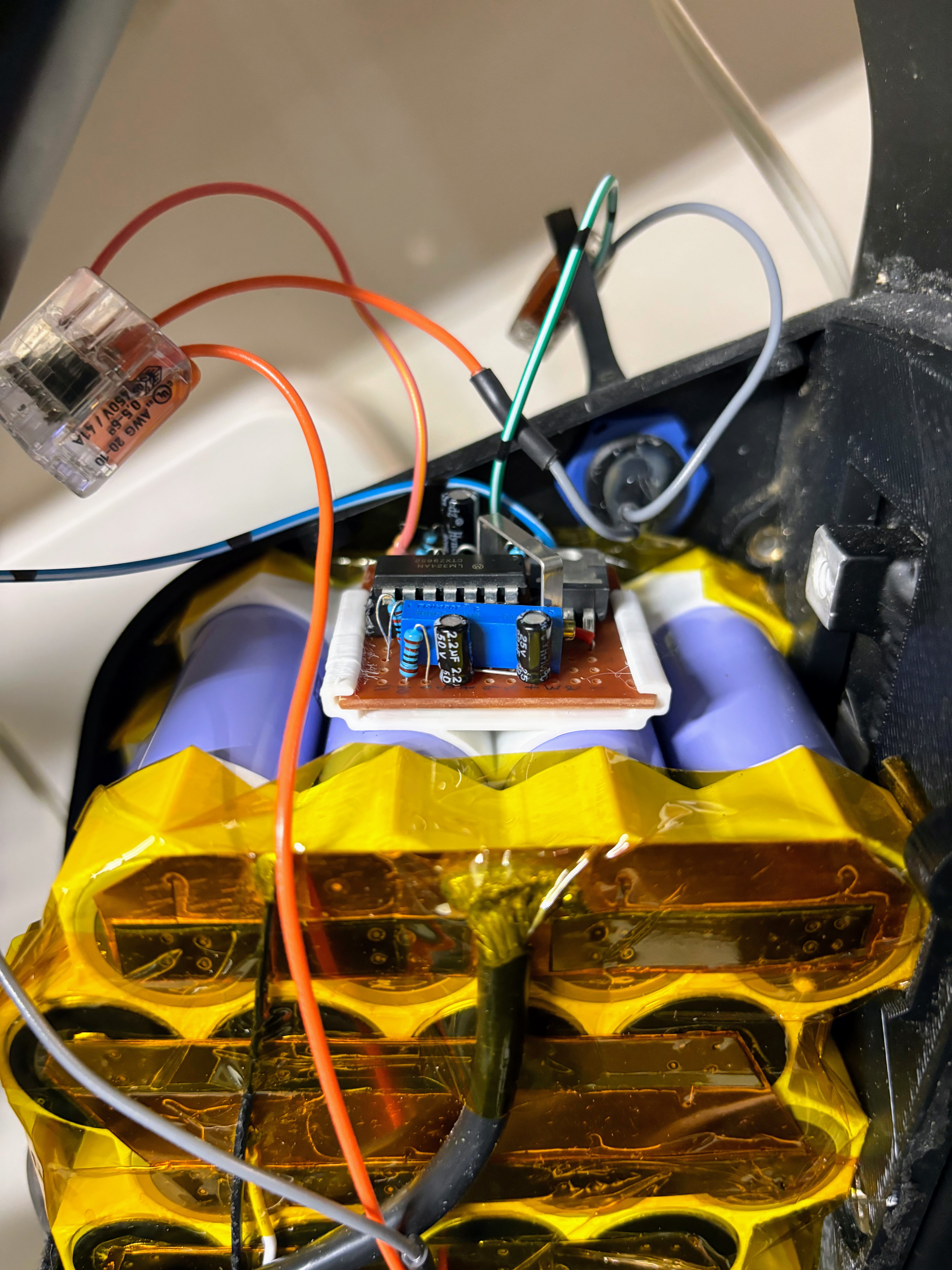
And here's the final implementation in a little 3D printed bracket, with 21700 cells for scale. The blue component is R9, I used a 10k trimpot that I had lying around.
Please note that if you want to build this circuit for a battery with a different voltage you'll need to adjust R10+R11 to keep at least 2mA flowing through the Zener diode D2. If your minimum battery voltage is VB, R10+R11 = (BV - 10) / 0.002
 George
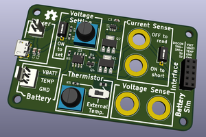
 James Fowkes
 Christoph Tack