 Marcel van Kervinck
This is a follow-up of my "Breadboard VGA from EEPROM" project that was covered here [hackaday.com] two weeks ago.
The video shows the new circuit's first signs of life. It is not really stable yet, but definitely getting somewhere. Halfway the build I changed the write-concept and to avoid having to start all over again some glitches are suppressed with 2 well-placed capacitors on signal lines.
More pixels and better colors
Because I do the X counter control now in a different way I have 6 bits available for color. So now we have 64 colors instead of 4-bits RGBI. The colors are also more vibrant by picking better resistors values for the DAC. I settled for 213x120 visible pixels (16:9), 8 MHz pixel clock, 31.25 kHz scanline frequency (32 us per scanline) and 59.5 Hz refresh rate. My LCD monitor matches the pixels nicely to its own 1920x1080 native grid.

The scope agrees with the new resistor values: red, green and blue VGA plug signals are seen here at 4 levels each from 0V to 0.7V. Perfect.
Software
The AVR/Trinket's job is to send pixels into the frame buffer. It does this through the shift register in the middle of the board to which it is connected by 3 wires. The 3 wires carry signals for a simple serial protocol: bitValue, shiftClock and commitToRAM. At the end of every scanline the TTL part performs a RAM write with the address and byte value taken from the shift register. If the Trinket doesn't update the shift register, the same write gets repeated every scan line, which becomes effectively a no-operation.
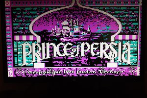
The Trinket is also limited in ROM, so it was a bit of a squeeze to get all the graphics and code in there. Almost all space, 90%, is eaten by the parrot image. The planet image piggybacks on the unused 2 bits in the parrot image. That leaves 3kB for the character set and code.
Only 6 bytes to spare! What to do with those?

Control signal generation
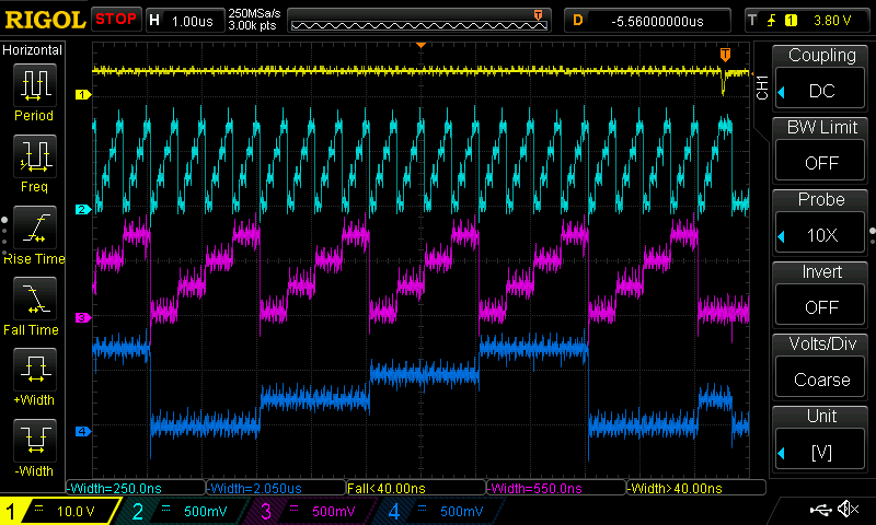
The X counter counts from 0 to 255 and then wraps around. This is different from the earlier project where I counted to 199 with a bit slower, 6.3 MHz, clock and sent a reset signal from the memory. As before, the VGA sync signals HS and VS come from memory in the same way as the color RGB data. Each cycle, one memory location gets clocked out. The last cycle is different: at that moment the current address and byte value from the shift register are written into memory. The trigger for this is the ripple carry out of the X counter (RCO). This pin goes high one cycle before the overflow. From this signal we derive the enable signals for the buses, the write pulse for the RAM, and we hold the clock into the flipflop for one cycle. This can all be seen in the trace below. From top to bottom:
- The RCO of the X counter highest 4-bits (74LS163).
- The derived write-enable signal for the SRAM. We want this only in the second phase of the cycle, because the address and value must be stable before write.
- The flip flop clock. One pulse is skipped to avoid leaking the write data that is on the bus into the VGA.
- The VGA color signal itself. The 4 last pixels of the scanline are visible at 4 levels.
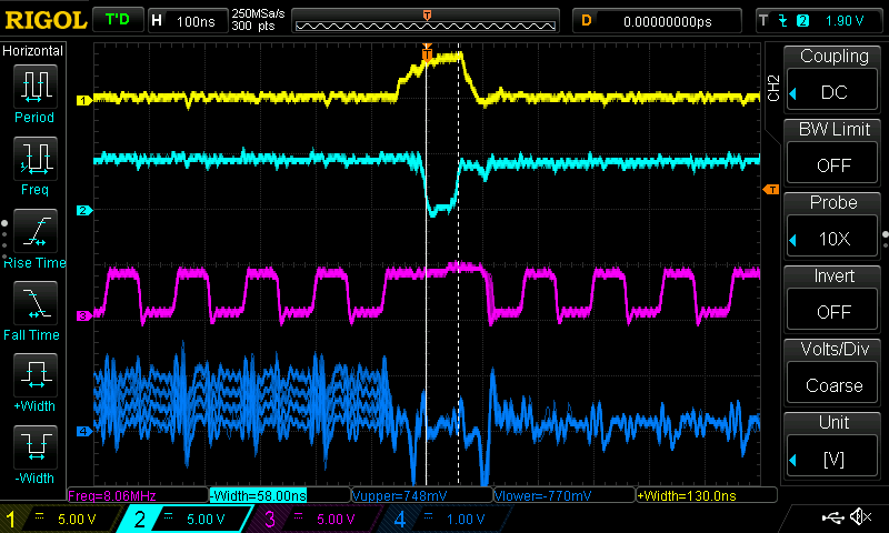
Glitches
The proper way to use RCO is through a flipflop, because it might be unstable before giving the intended value. In fact there is a brief glitch 16 cycles before the overflow from 255 to 0, originating from the low order X counter RCO (see the purple [inverted] trace below). I now suppress this with the 330pF ("331") capacitor.
Similarly, because during cycle 255 the Y ROM is not on the bus, its Y counter reset signal (D0 out) is temporarily invalid. This gap is bridged with a 0.1µF ("104") capacitor. This works because the EEPROM's D0 isn't connected to the bus.
Two somewhat ugly hacks, but good enough for me for now.
The shift register is made out of 74HC595 chips, the same chips used in the offline EEPROM programmer. While shifting in new data they keep emitting the old value to the bus, so there is no worry there for putting garbage into RAM. There is one catch however: there is no synchronisation...
Read more »
 Nick Bild
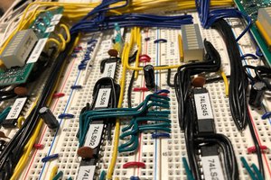
 Ced
Ced
 teardownit
 Keith
Keith
Do you have a schematic of the board?