 Chris.deerleg
Simulation
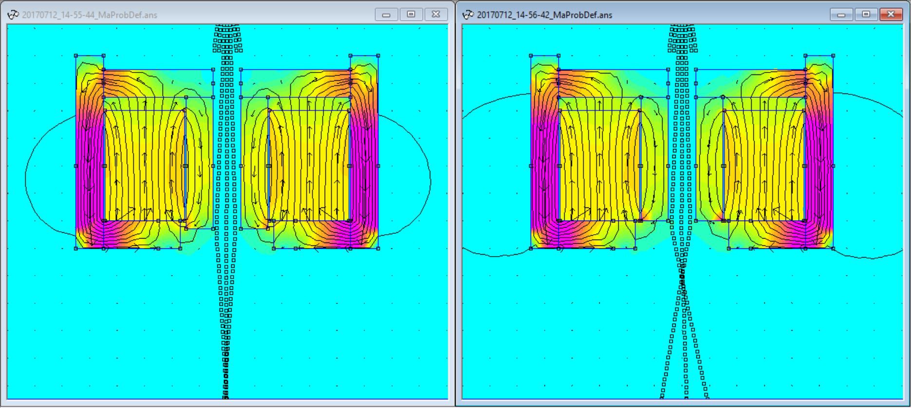
A Simulation is available since the Log 07/13/2017
Magnetic lens system Vacuum and electron beam
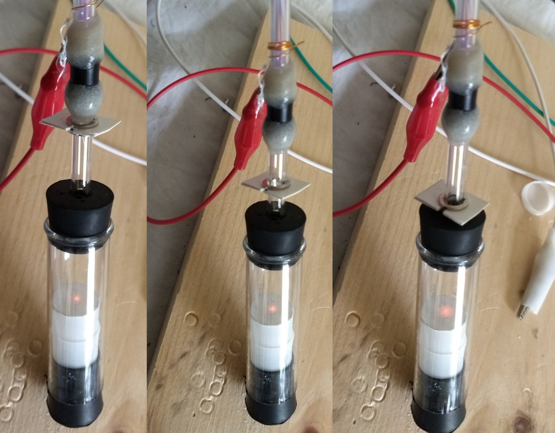
I have a magneticlens system since 11/06/2017
Housing
Since 12/28/2017 I have a improved housing

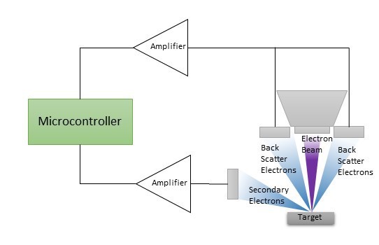
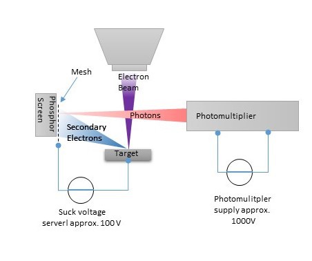
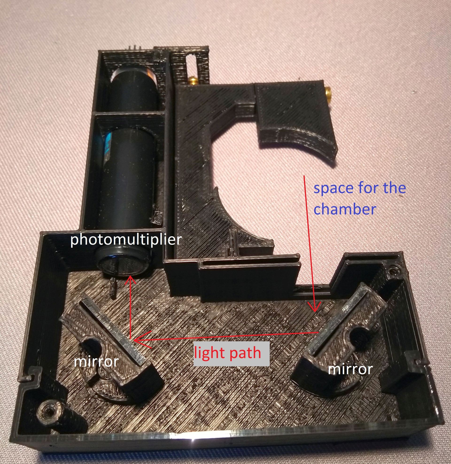
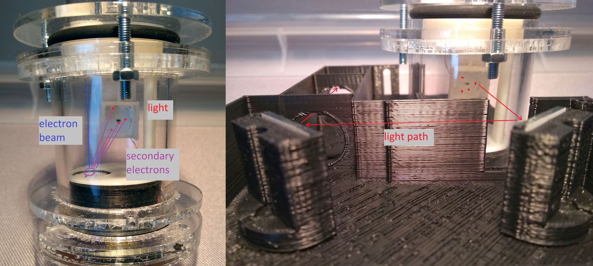
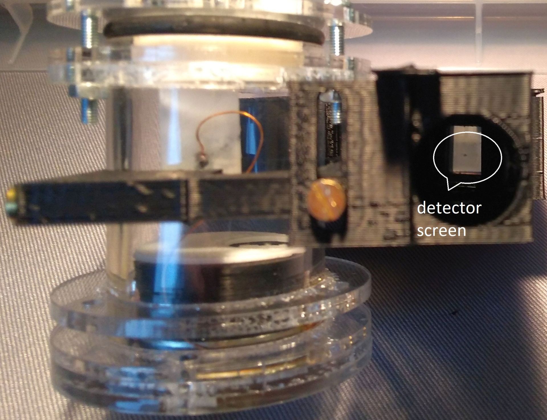
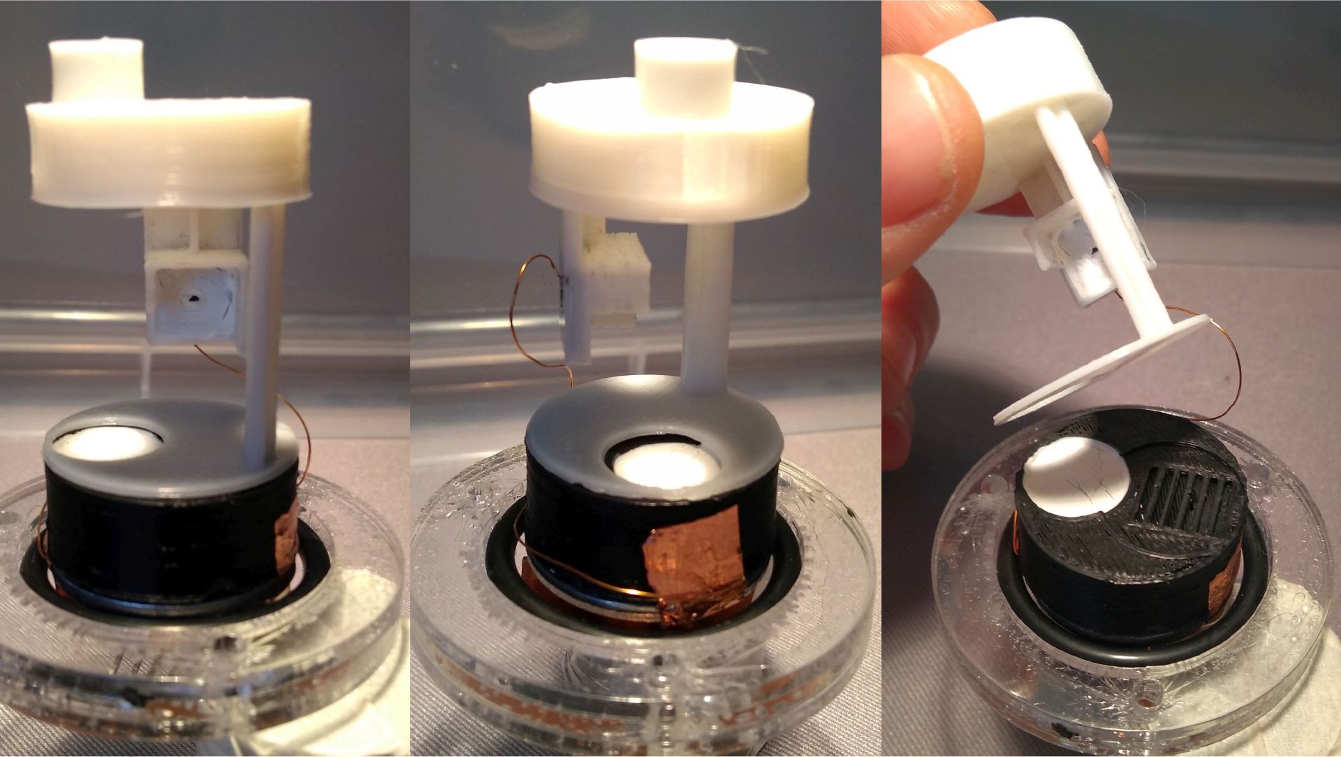
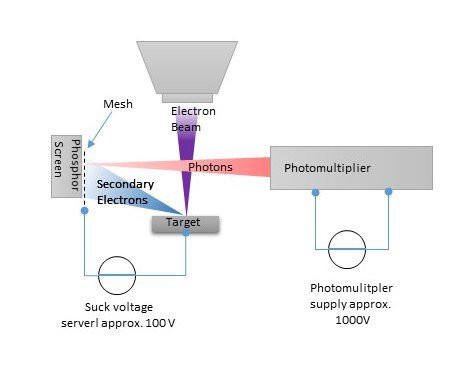
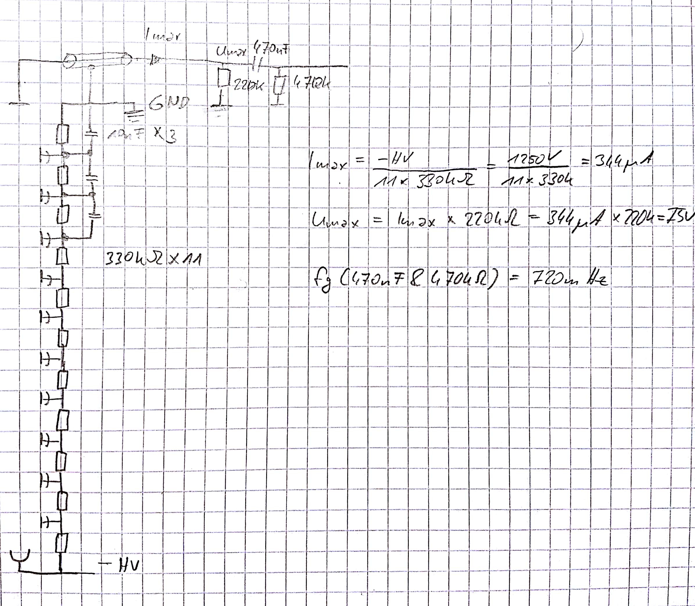
Electron detector
I have a schematic since 02/21/2018 for the detector amplifier
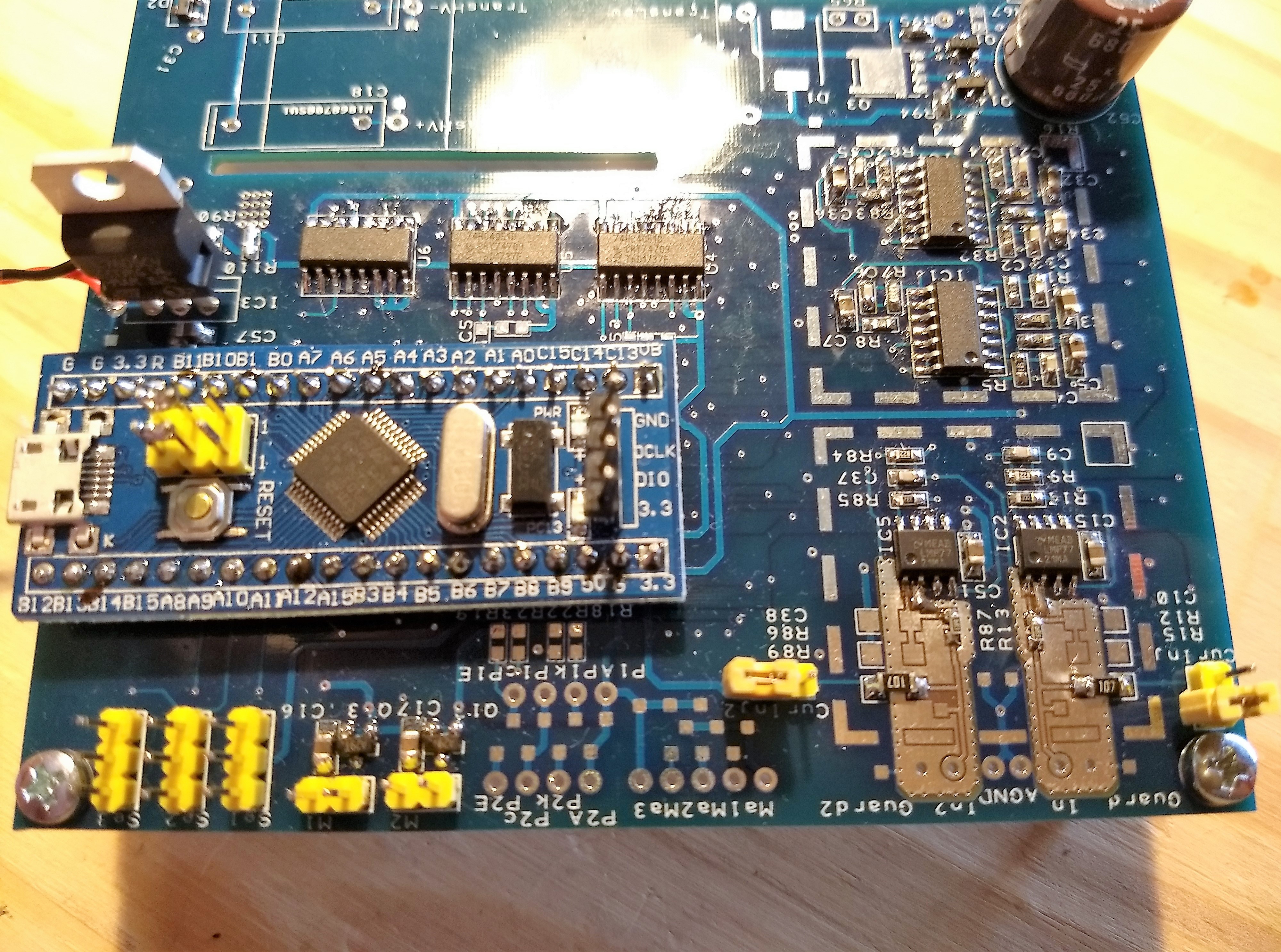
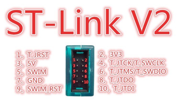
High voltage shield for Arduino
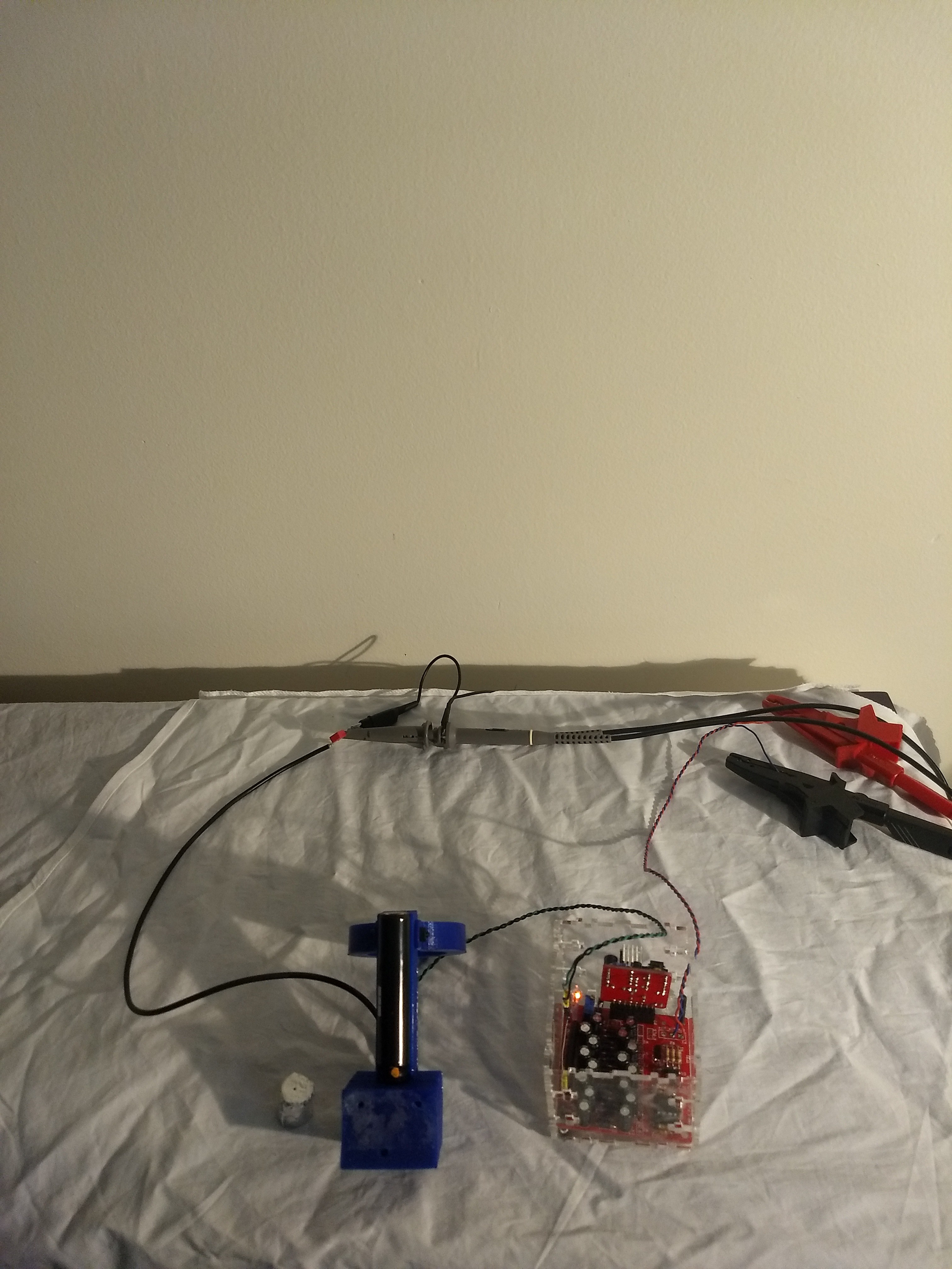
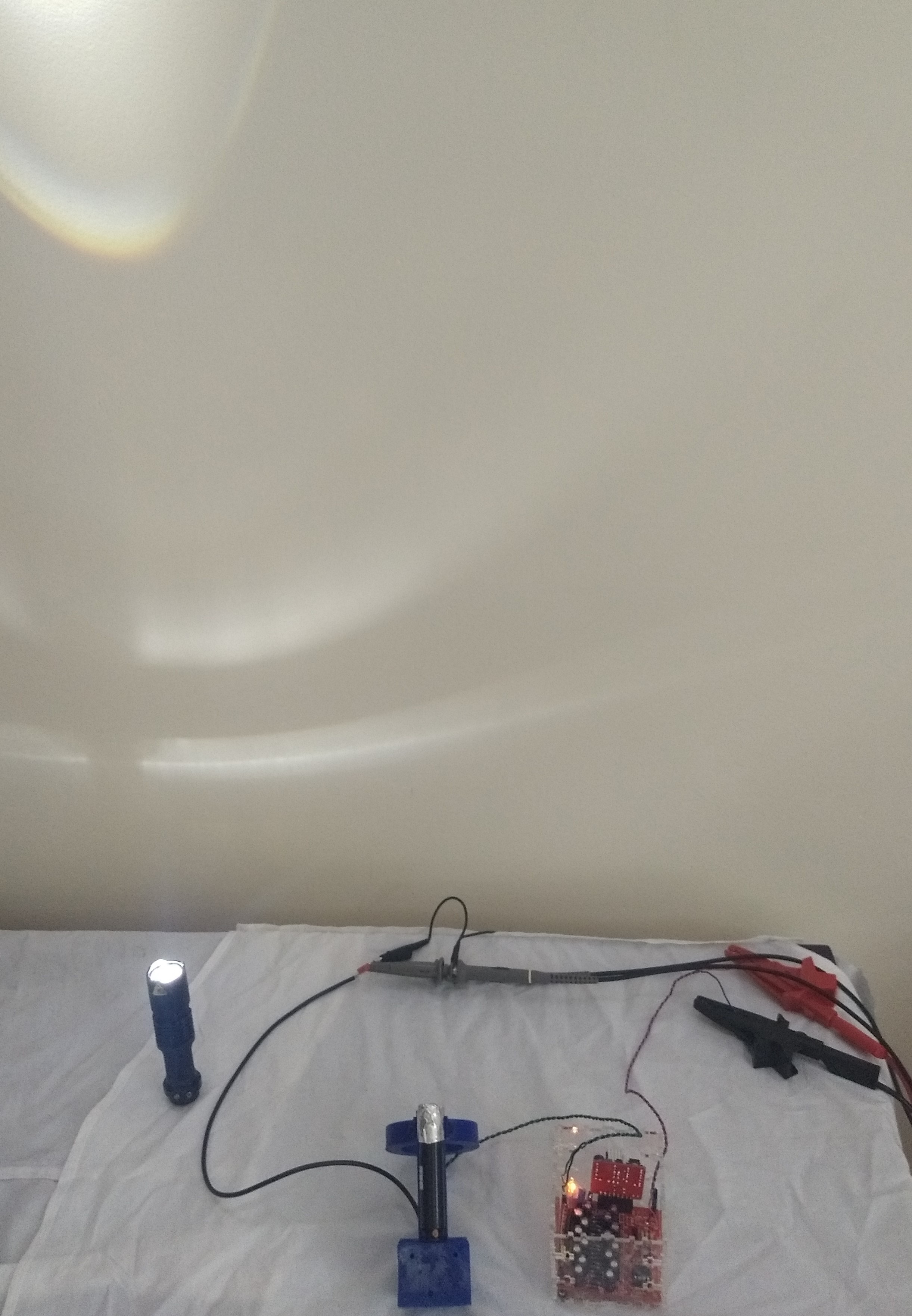
I populated the bare PCB about 03/16/2018
Overview and Introduction of SEM
1965 was the first Scanning Electron Microscope (SEM) commercially available (wiki). 2011 Ben build the first SEM at home. He used special equipment to build it. Now 2017 I start to build the first SEM with common available components. I would like to create imanges like these.


I will not explain the principles of a SEM because the explanation on the homepage of ammrf.org.au is great and I can't do it better.
Also the overview video from Ben is great for the introduction. But for a deep understanding I recommend the book Physical Principles of Electron Microscopy from author Ray F. Egerton.
My plan is to go ahead with the following steps:
- Simulation
- Vacuum and electron beam
- Housing
- Magnetic lens system
- Electron detector
- High voltage shield for Arduino
1. Build a simulation with a magnetic field simulation tool to determine the dimensions
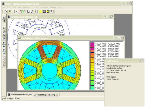
I want use the tool FEMM 4.2. This tool is free and it is possible to create code based on Lua 4.0.
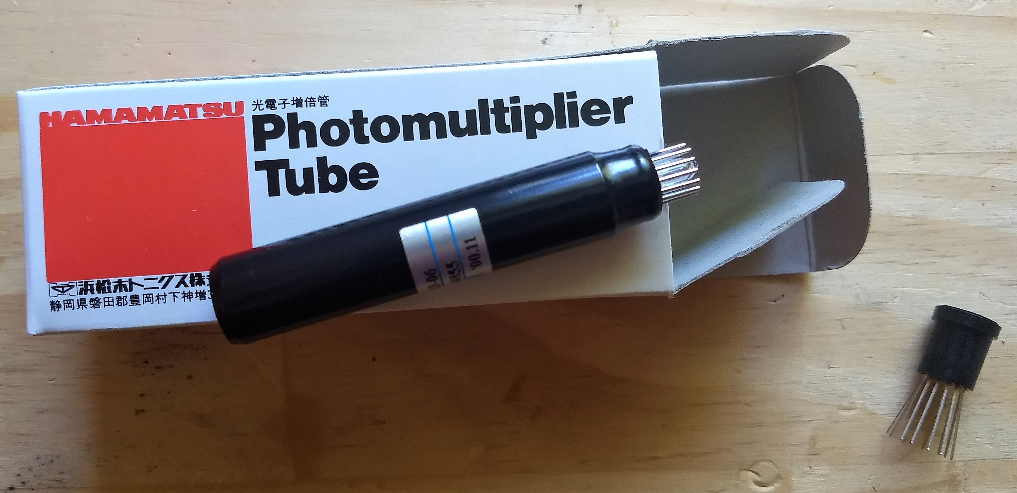
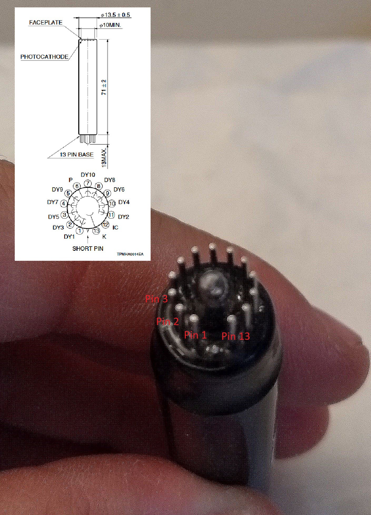
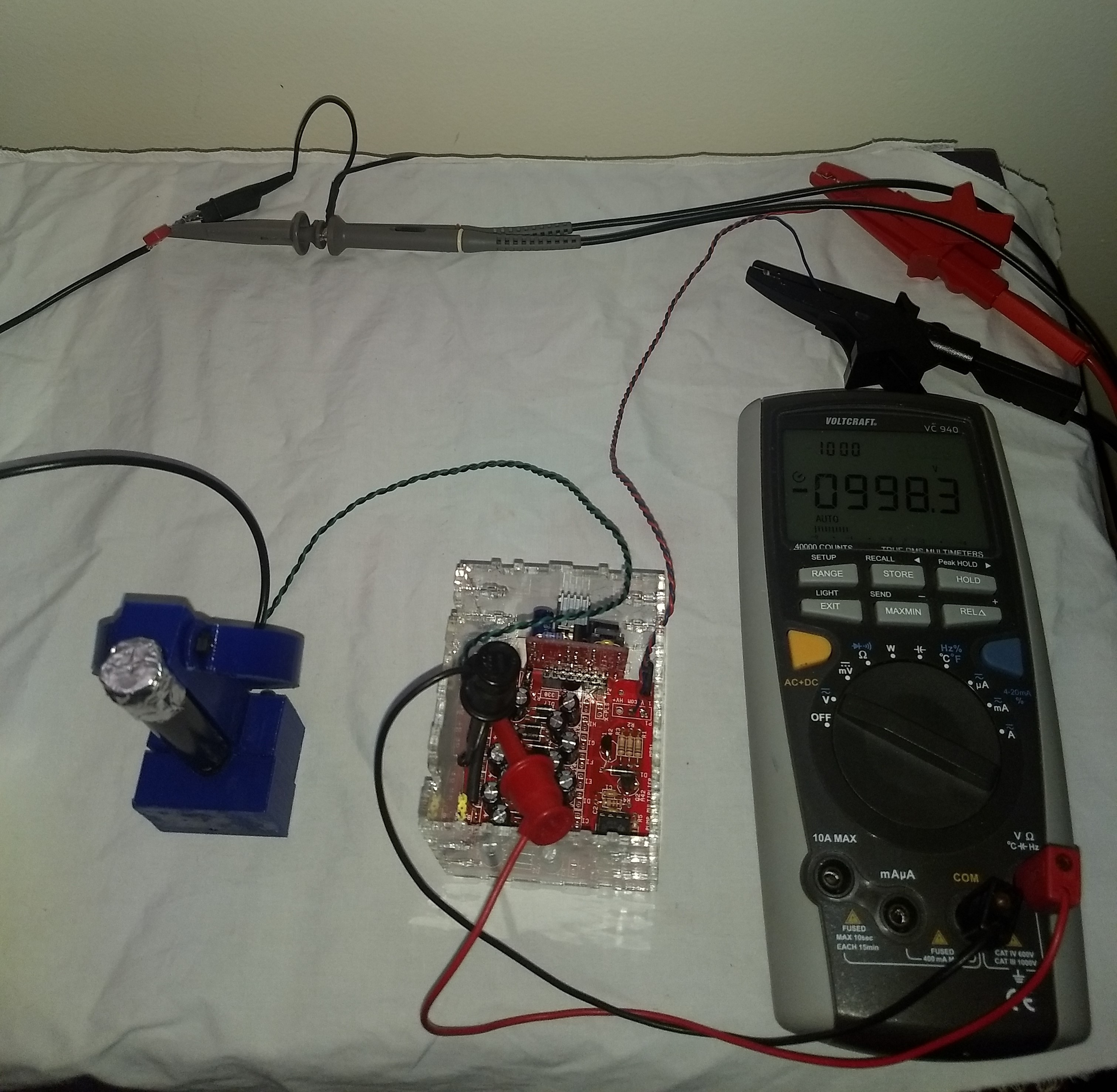
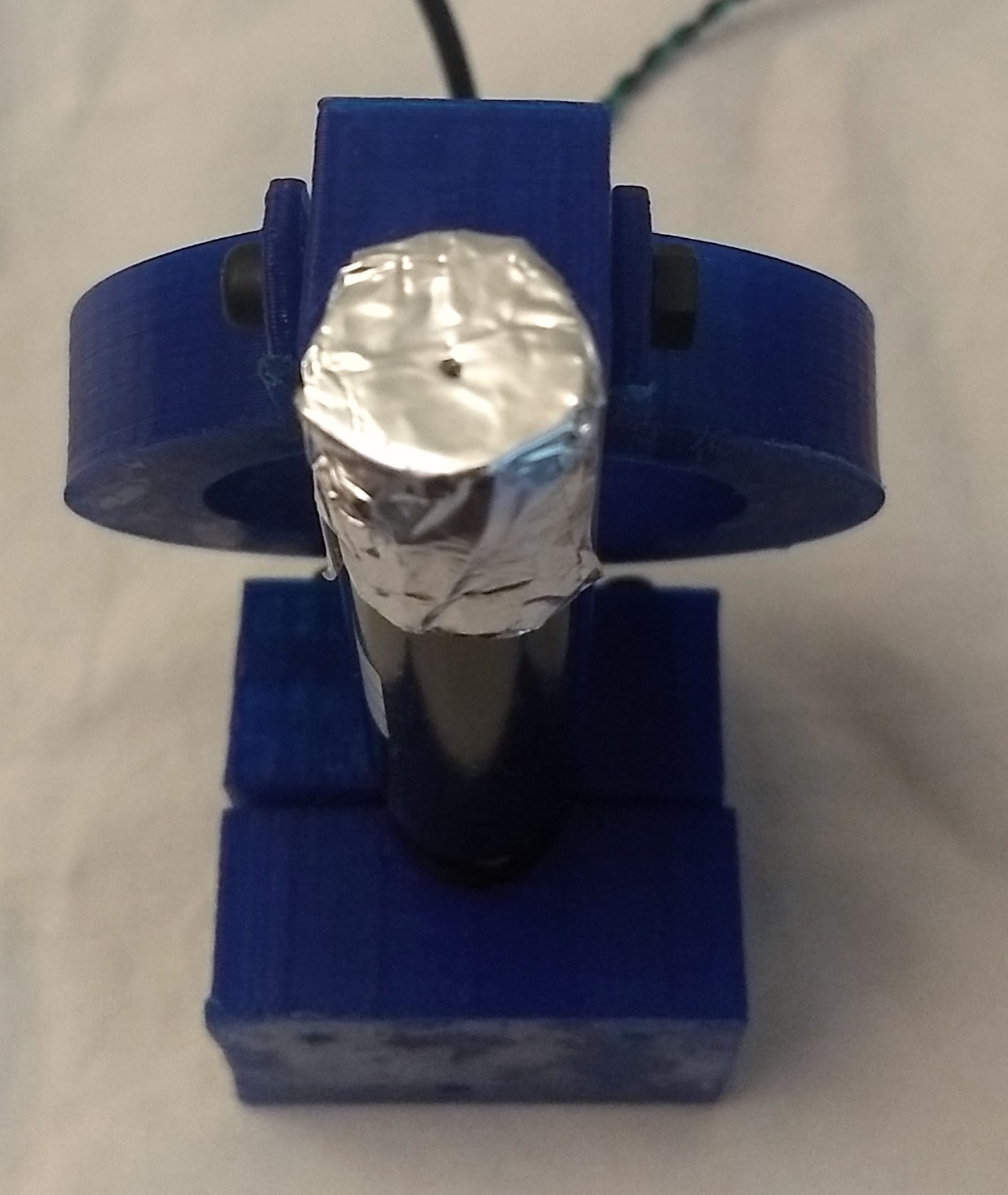
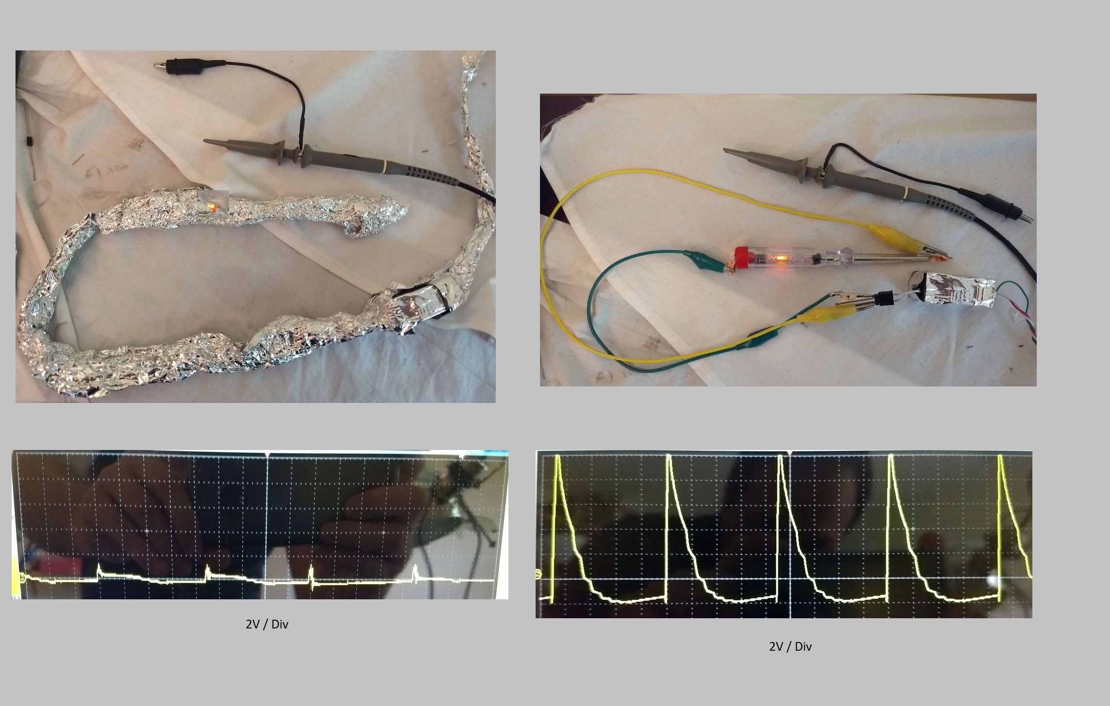
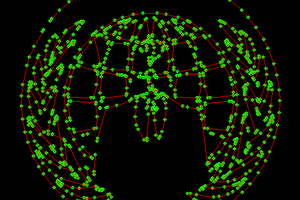
 One of my first test was just to point the photomultipler to the wall and illuminate it with my desk lamp. In this test I figured out that i need an aperture.
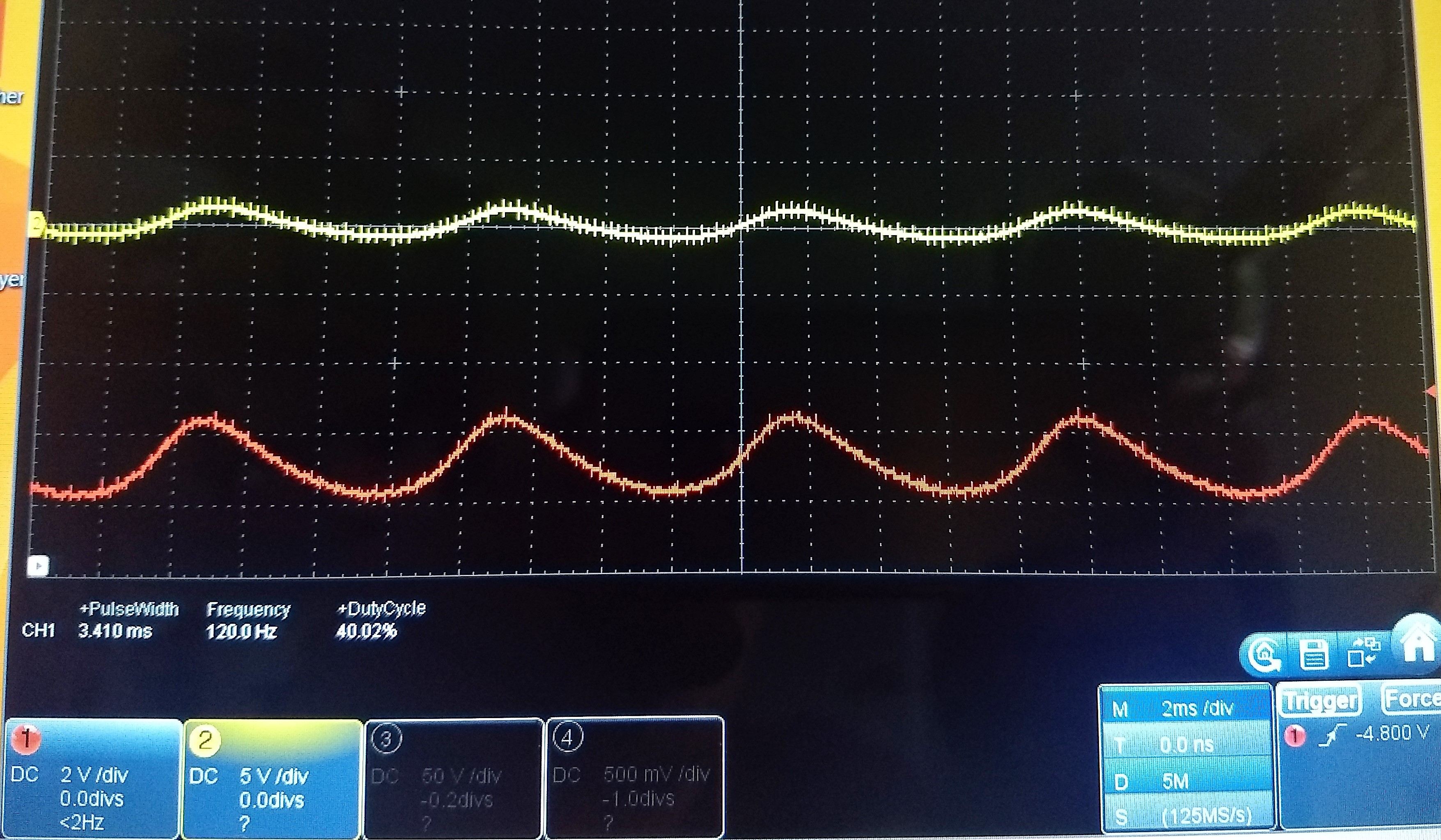


 The image above visualize how the buffer content looks like. The buffer contains random data like "BEEF.." then transmit the micro controller a header like "480 Hello_World" and the data of for example ADC chanel1 and ADC channel 2 in a 16 Bit format.
  The image above shows how the buffer look like after run the line of codes.
 The image above shows how the buffer look like after run the line of codes.
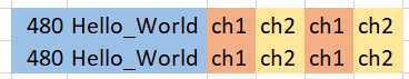 The image above shows how the buffer look like after run the line of codes.
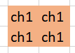


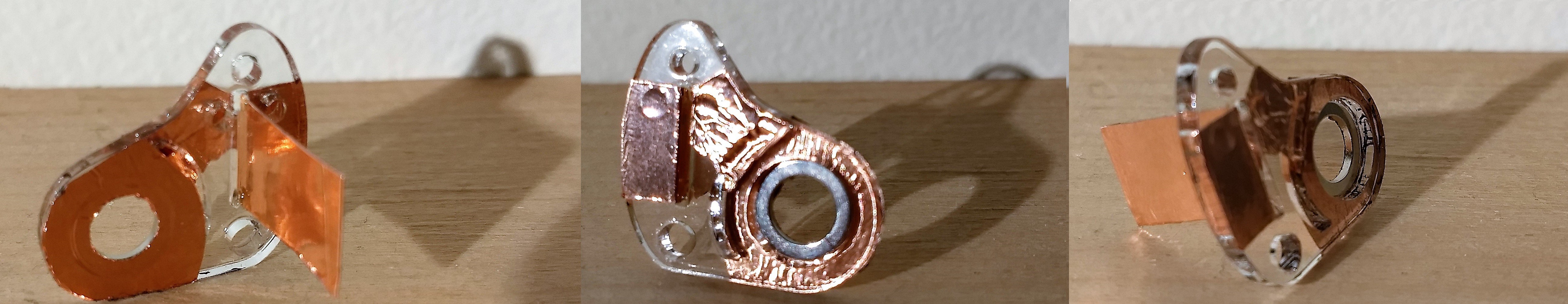
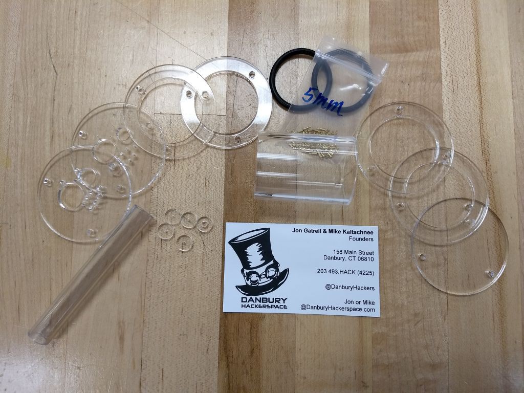 I decided to make a new chamber because I need more space in the chamber that I can begin to build the electron detector. In the image above are the single parts of the chamber shown. The parts are made of 3mm acrylic sheet. The 5mm golden pogo pins are from Ebay and the black rubber rings are from sealing kit from Amazon.
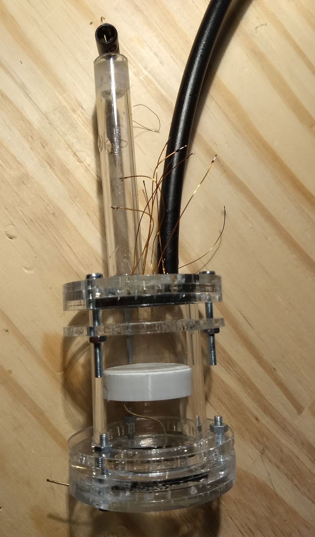
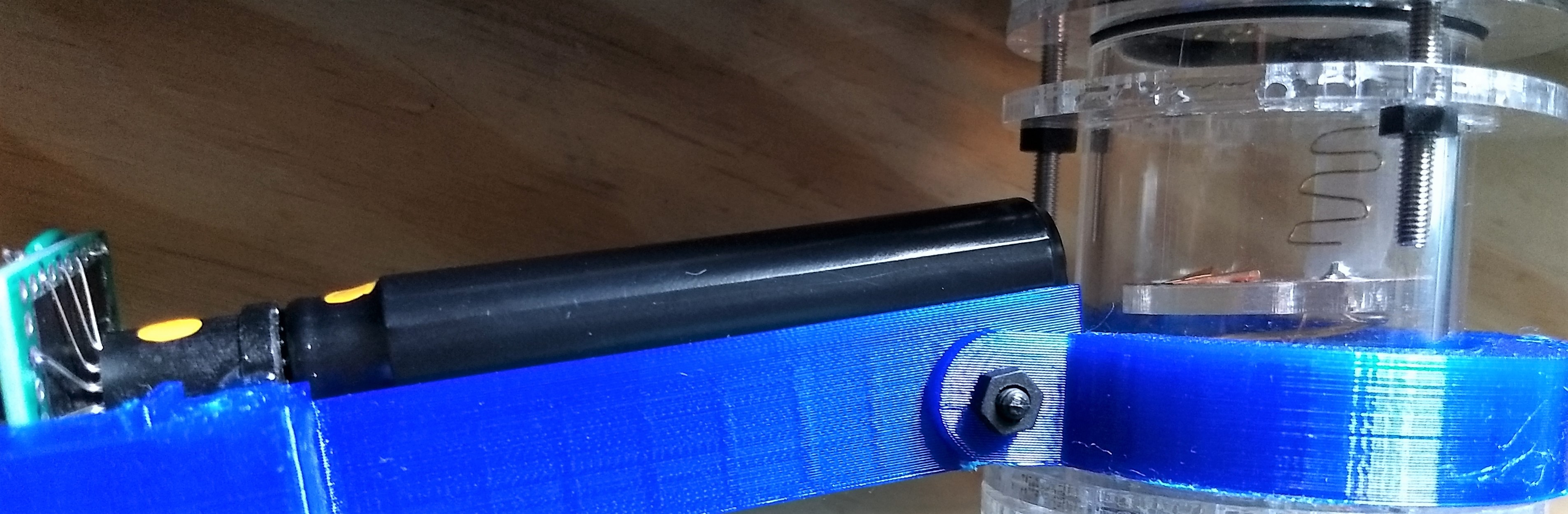
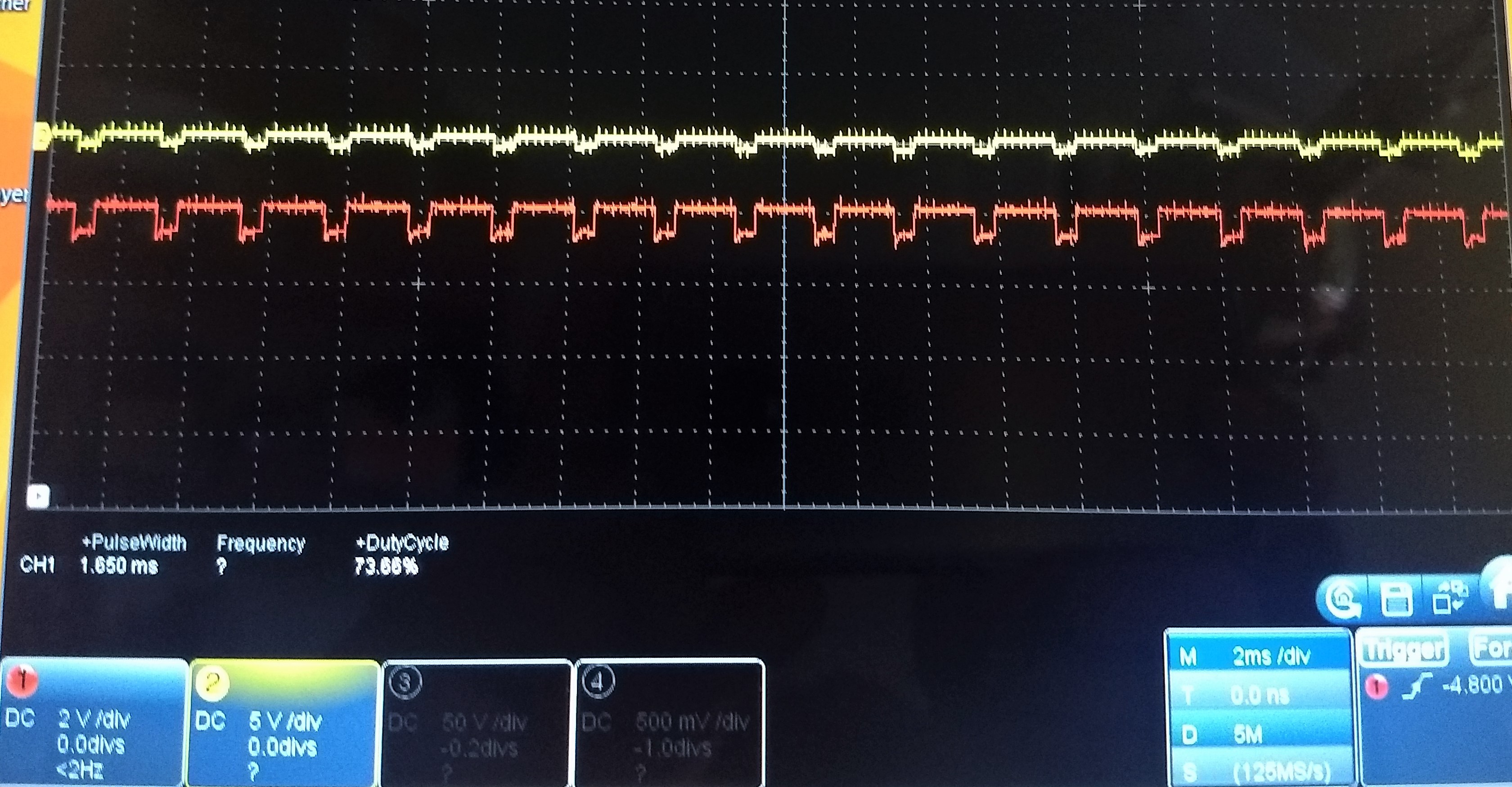
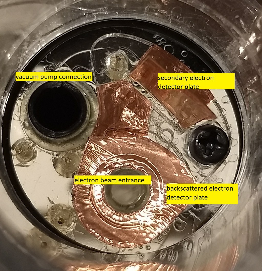
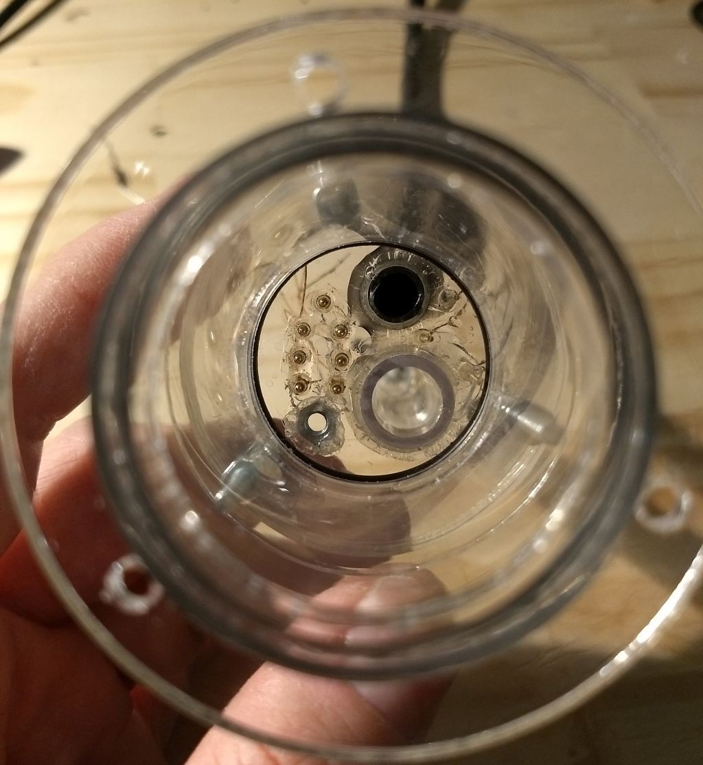 On the image above are the connections in side the chamber shown. The black tube is the connection to the vacuum pump. The clear tube below is the entrance for the electron beam. Left to the tubes are the pogo pins and a nut. These elements should connect the electron detector to the outside. On right side are three pegs visible. With these pegs I want to measure the vacuum because I had a lot of trouble with the vacuum in the past.


 danjovic
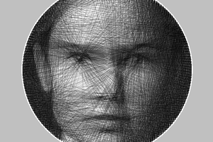
 rawe
rawe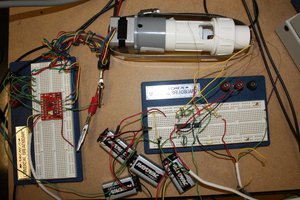
Wow, your project is such a great. As I have learned something new by reading this project. Would like to share it with the team members of https://lemotwordle.com/ so that they could also read it and can implement something new in our running projects.