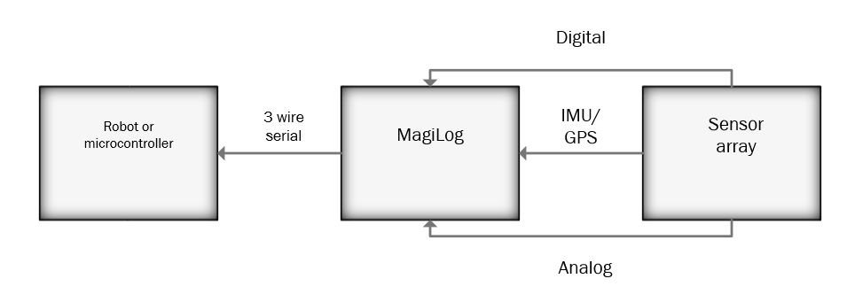
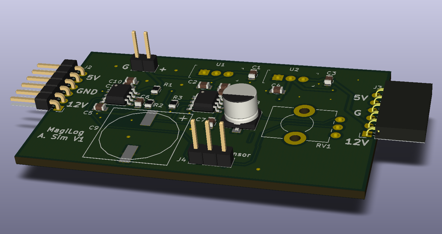
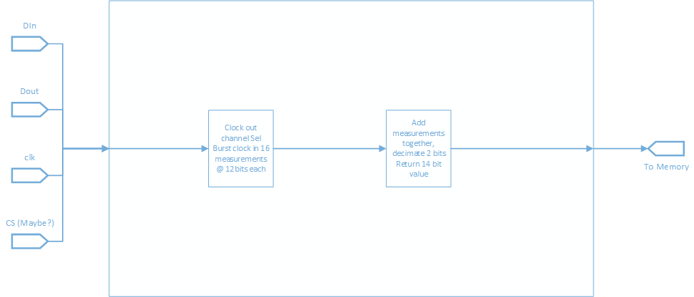
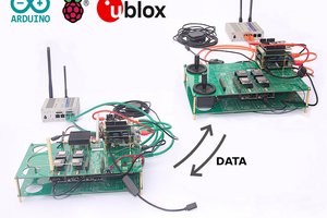
Close
0%
0%

MagiLog: Open Automotive Datalogging

Developing a full featured datalogger on the cheap

Similar projects worth following
In motorsports there is no such thing as too much data. With data, drivers can review their inputs to improve consistency and lap times. Unfortunately, for a quality motorsport oriented datalogger you are looking at spending thousands of dollars. I think I can do it cheaper.

I started researching how to make a high functionality automotive DAQ about 5 years ago but never got around to building it. What came from that was the idea for the MAGIc LOGger. I'm hoping to go over my old work, refresh some components, and get a working device out in 2018.

The MagiLog will have analog/digital I/O for interfacing with automotive sensors, built in GPS, IMU, Bluetooth and SDCard support. Not only will it interface directly with sensors, it will be able to read data from the ECU via CAN, OBD and serial. It will be based around a Spartan-3 FPGA for the I/O and the communications/logging will managed by the XMEGA A1U microcontroller.

MagiLog is an automotive focused datalogger that is based on an XMega/FPGA coprocessing configuration. The XMega and the FPGA communicate with each other through dual-port RAM. This will allow me to access the FPGA as an extension of the XMega’s memory space through the External Bus Interface (EBI) and then use the DMA controller to send the data to the various communication methods with little overhead. I think this arrangement will allow me the greatest flexibility when it comes to scaling up the design and allowing me to exceed my initial target of 100Hz datalogging.

My initial target specs and capabilities are as follows: MagiLog will have 16 analog inputs to interface with various sensors directly. It will have 12 inputs for digital inputs, these inputs can be used to track engine RPM or any toggleable parameters. MagiLog will also have an integrated 9 axis IMU with GPS combined with a Kalman filter or some other sensor fusion algorithm for accurate kinematic tracking. In addition to the direct sensor interfaces, MagiLog will also be able to acquire data from an engine control unit (ECU) through either serial or CAN/OBD protocols.

The logged data can be saved to an SD Card or streamed to another device/computer over Bluetooth and USB.

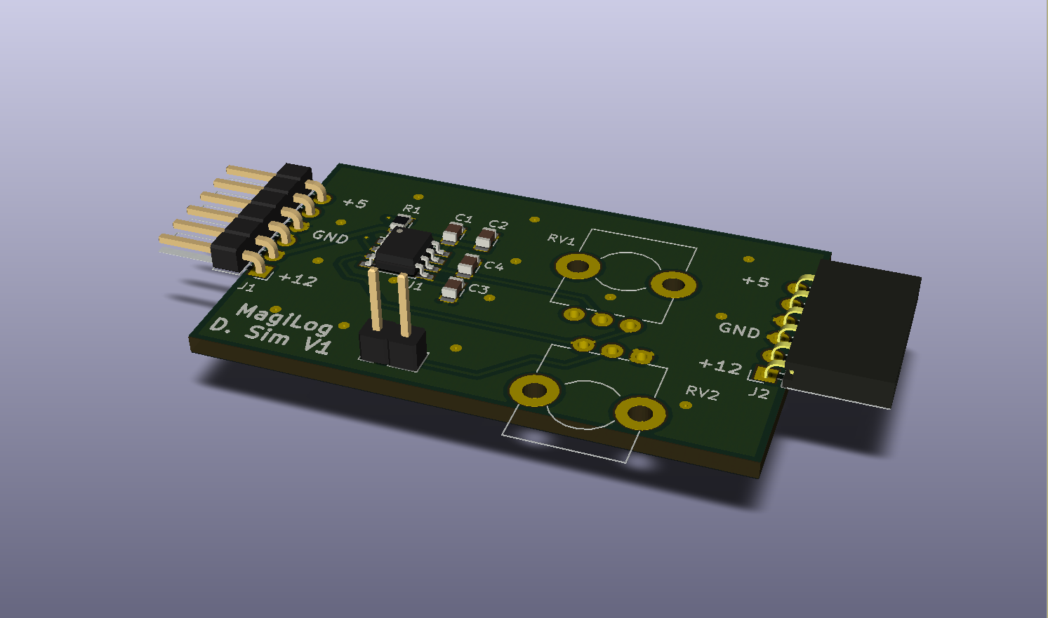
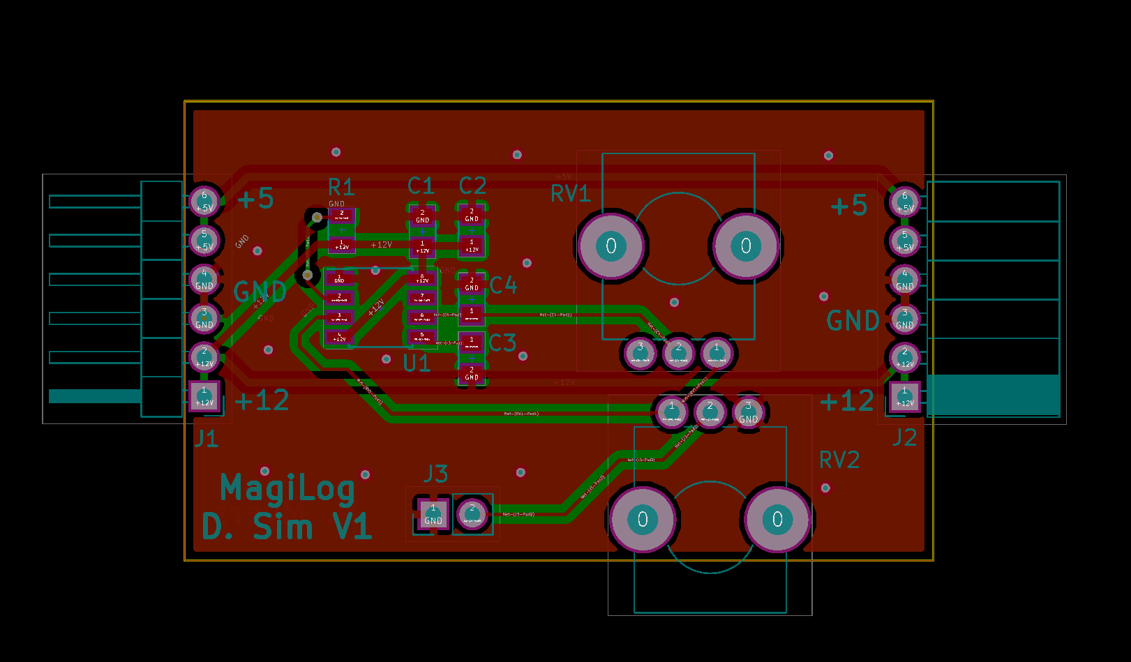
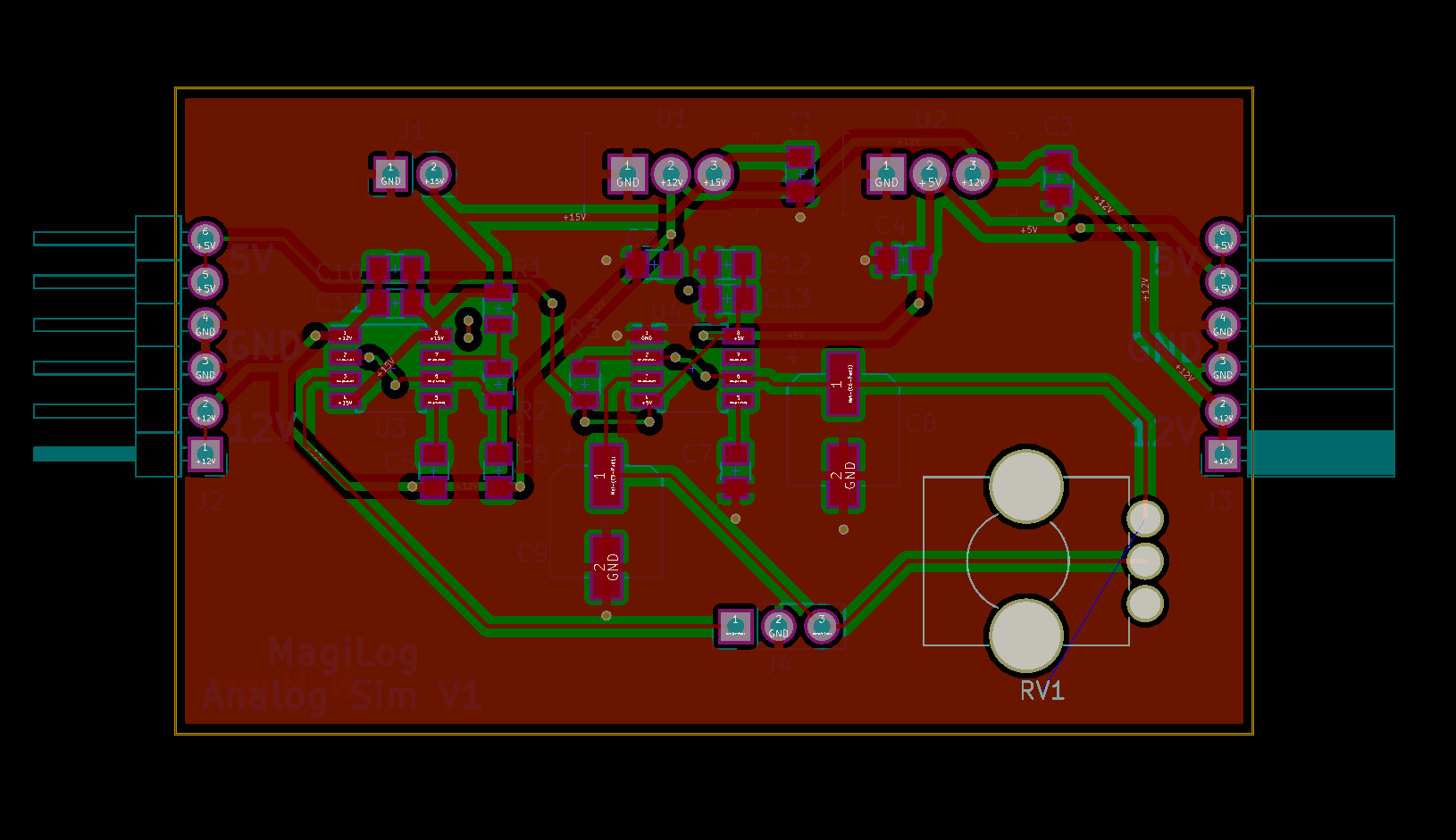
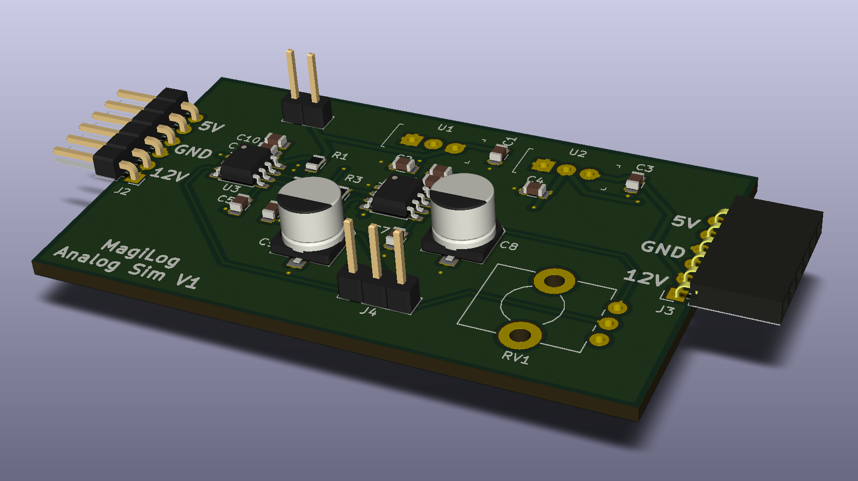
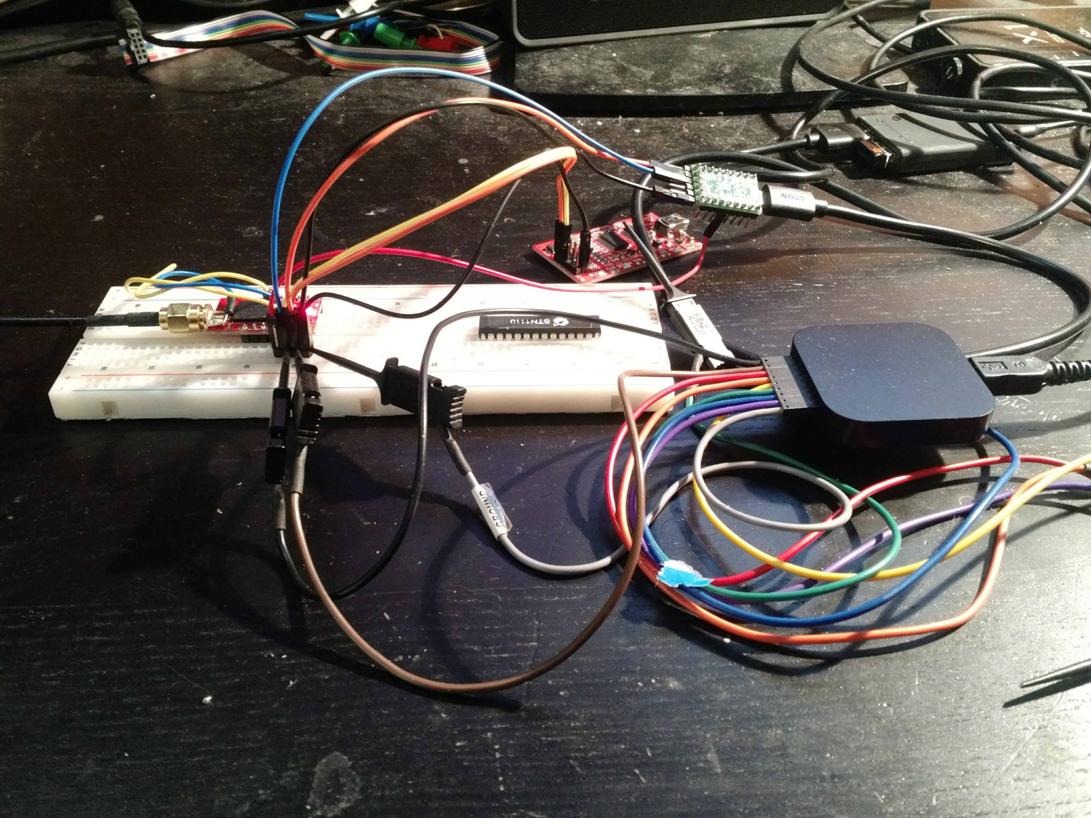
I have all the components specced or respecced and am now getting into the HDL/programming side of things to integrate all the components together. Once that’s done it’ll be time to roll a PCB to get everything on a single board.

For long term expandability it will also have an auxiliary serial port to allow you to eventually add displays or interface with MagiLog with a robot or any other application that can accept a serial data stream.

I’m hoping through the creation of this project page I’ll improve the way I document projects and maybe as a bonus I can teach people how to use the tools I am using to complete this project.

Banner photo from Wikimedia

DigitalMaster.zip

HDL files for the FPGA digital module.

application/x-zip-compressed - 1.55 MB - 05/25/2018 at 01:00

Download

Digital Sim.zip

PCB files for the digital simulator

application/x-zip-compressed - 34.11 kB - 05/25/2018 at 01:00

Download

Analog Sim.zip

KiCAD PCB Files and Digikey BOM for Analog Simulator

x-zip-compressed - 60.36 kB - 05/20/2018 at 04:13

Download

ADC.zip

ADC Module HDL and testbench

x-zip-compressed - 2.44 MB - 05/20/2018 at 04:12

Download

DigitalSim.asc

Spice for digital sim

asc - 1.69 kB - 04/03/2018 at 21:56

Download

View all 6 files

  • 1 × Spartan 3AN Starter Kit Main I/O backbone
  • 1 × XMEGA A1U Xplained Pro Communication and high level tasks
  • 1 × Microchip RN42 Bluetooth Module
  • 1 × Microchip MPU9250 9 Axis IMU
  • 2 × TI ADC128S022 ADC

View all 7 components

  • Module Magic (Via the Second Serial Port)

    Nigel06/04/2018 at 05:44 0 comments

    Seeing how this round is the Robotics Module round I suppose I need to explain how you could use MagiLog as an integrated data collection module for a robot. In addition to the serial port used to communicate with ECUs there is an auxiliary serial port for bidirectional communication between accessories or another microcontroller.

    One kind of accessory I’m wanting to specifically develop is a digital dash display. Something like what you could get from Motec, except at about 1/10th the cost.

    As a module I’d like to be able to set a mode where MagiLog either streams through selected data values or have it work as a request/response type system. Either way it’d allow you to connect a wide range of digital inputs, analog inputs, and IMU/GPS data to your robot using only 3 wires. Ground, MOSI, and MISO. Since this would also be working through DMA I’d imagine with some optimization work we should be able to maintain a very fast refresh rate. 

  • Digital Module HDL

    Nigel05/27/2018 at 23:28 0 comments

    Last weekend I was able to finish the HDL for digital inputs. The system comprises of 2 modules I’ve written and one pre-built IP. As with the other modules, each word of data will be 16 bits. I’ve chosen the following encoding scheme:

    As you can see the MSB is the status bit, it is high when the input is high. The other 15 bits then are left to act as our counter. We won’t be directly calculating frequency/RPM, but the time between pulse events. As this means we need a division step we end up with nonlinearities in the resulting data. As we get closer to a single clock cycle, the read frequency gets very large and the gap between steps also grows. Because of this we need to carefully consider what clock rate we want to use as the timing input. After some playing around I ended up deciding on 250kHz. This gives me a max RPM of 18750 and a minimum of 457.8. The following graphs are cut off at 800 counts for readability. Also, the corresponding frequencies below 800 counts are higher than we probably would ever need.

    Now onto the actual HDL I’ve used/written. The counter IP is configured as follows.

    The digimodule module is the data collector for each channel, it times the gap between pulses and directly connect the pulse state to the state bit. Outside of the timer it’s pretty simple, there’s a one-shot pulse generator to clear the counter and another flag to denote when we’ve hit overflow.

    `timescale 1ns / 1ps
    //////////////////////////////////////////////////////////////////////////////////
    // Company: MagiLog
    // Engineer: Nigel Myers
    // 
    // Create Date: 05/17/2018 03:25:31 PM
    // Design Name: Digital Input'
    // Module Name: DigiModule
    // Project Name: MagiLog 
    // Target Devices: 
    // Tool Versions: 
    // Description: 
    // 
    // Dependencies: 
    // 
    // Revision:
    // Revision 0.01 - File Created
    // Additional Comments:
    // 
    //////////////////////////////////////////////////////////////////////////////////
    
    
        module DigiModule(
        input wire signal, //Module I/O definitions
        input wire clock,
        output wire status,
        output reg [14:0] data
        );
        
        wire [14:0] q; //Counter output wire 
        wire thresh; //Threshold notifier
        wire sclr; //Counter clear
        reg r1, r2, r3; //Single pulse registers
        reg flag; //overflow flag
        
        c_counter_binary_v11_0_0 DigiCount ( //Counter module
          .clk(clock), // input clk
          .sclr(sclr), // input sclr
          .thresh0(thresh), // output thresh0
          .q(q) // output [14 : 0] q
        );  
        
        assign status = signal; //Continously assign status state to signal level
        assign sclr = r2 && !r3; //Get one pulse out of sclr
       
        always @(posedge thresh or posedge sclr) begin //Overflow and clear routines
            if (thresh)
                flag = 1'b1;
            else if (sclr)
                flag = 1'b0;
            else
                flag = flag;
        end
            
            
        always @(posedge signal) begin //At every signal posedge, we check time since last pulse
            if (flag) begin
                data = 15'b111111111111111; //If data overflowed we use max value as notifier
            end else begin
                data = q;
            end
        end
         
        always @(posedge clock) begin //Pulse generator for sclr
            r1 <= signal;
            r2 <= r1;
            r3 <= r2;
        end
                     
    endmodule
    

    The top-level module consists of a state machine with states for each channel, as well as an idle and send state. During the send state, we set the correct module output and associated address and pulse a write request to SRAM.

    module DigitalMaster(
        input wire [9:0] SigIn, //Signals into module
        input wire trigger, clkSlow, clkFast,  //Record trigger, main clock, and timer clock
        output reg [15:0] dOut, //Data output
        output reg [3:0] adrOut, //Output address
        output reg write_en //Ram Write Enable
        );
        
        wire [15:0] dataMux[9:0]; //Mux for counter module outputs
        reg [3:0] cstate; //State trackers
        reg [3:0] nstate;
        reg [3:0] nnstate;
        
        localparam [3:0]  //Channel addresses
            Ch0 = 4'b0000,
            Ch1 = 4'b0001,
            Ch2 = 4'b0010,
            Ch3 = 4'b0011,
            Ch4 = 4'b0100,
            Ch5 = 4'b0101,
            Ch6 = 4'b0110,
            Ch7 = 4'b0111,
            Ch8 = 4'b1000,
            Ch9 = 4'b1001,
            Send = 4'b1010,
            Idle = 4'b1011;
        
        DigiModule Chan0 ( //Instantiate 10 modules
     .signal(SigIn[...
    Read more »

  • Digital sim PCB done!

    Nigel05/25/2018 at 00:59 0 comments

    The PCB for the digital input simulator has been done for a bit now. Had some other things that I needed to take care of, so this log got pushed back a few times. I ended up finishing only a day or two after starting, in part to it being a much simpler board than the analog sim. I’ve uploaded the newest round of files to the project page. I should move everything to Github at some point. Perhaps towards the end of the month I’ll have some time to set that up.

    The circuit is based around a single 555 with 2 control pots. One of the pots handles the output frequency, and the other pot handles the amplitude of the pulses. (See older log for more details) This lets us easily adjust the voltage and frequency of the inputs to the FPGA. Using an oscilloscope, I can verify what the FPGA is recording to make sure things are good with the HDL and hardware. The code for the digital module is done, I just need to finish commenting the code as well as the associated project log. There ended up being more details worth discussing than I originally thought so it’s taking a bit of time. Hopefully I’ll have it out in the next few days.

  • Weekend Update

    Nigel05/20/2018 at 04:11 0 comments

    I was able to finish the analog module HDL as well as the digital simulator PCB. I’ll expand more on the latter tomorrow, but I’ll go over the ins and outs of the code used in the analog module in this update. The point of this module is to interface my chosen ADC on one end, and produce data and ram write requests on the other. This module in the end will be a few levels down from the top as we need to combine the data from disparate modules into a single address space that we can access from the XMega.

    The analog module is comprised of 4 main parts, which I will cover individually: The top-level module, the process controller, the data shift register, and the accumulator. With these 4 components I can interface with my ADC which produces 12bit measurements and combine multiple measurements into a new 14bit measurement for each channel. These measurements are then ready to be saved in some variety of RAM to be accessed by the XMega.

    The top-level module is quite simple, it contains the modules needed for each ADC and maps the appropriate I/O for the data to be recorded. One thing to note is we get around the need for a separate bit shifting step by forcing the two MSB to 0 and then discarding the two LSB to get the 14 bits of data we care about.

    module ADC_Master(
        input wire clk, // ADC clock in, 8MHz nominal
        input wire trigger, //Update cycle trigger signal
        input wire MISO, // Master In, Slave Out
        output wire MOSI, // Master Out, Slave In
        output wire sclk, //Clock output to ADC
        output wire CS, //ADC Chip select line
        output wire [2:0] adr, //Address to write data to
        output wire [15:0] data, // Data to be written
        output wire w_en // Write enable for data
        );
        
        wire shift_en, done; // Shift register status comms
        wire add, rst; //Accumulator control lines
        wire complete;
        wire [15:0] acc_in;
        wire [15:0] acc_out;
        wire [2:0] chan;
        
        assign data = {2'b00, acc_out[15:2]}; //Bitshift 16 bit sum to get 14 bit data
        assign w_en = complete;
        
        spi_shift shift ( //SPI Shift register module
            .sclk(sclk),
            .MOSI(MOSI),
            .MISO(MISO),
            .CS(CS),
            .clk(clk),
            .done(done),
            .shift_en(shift_en),
            .chan(chan),
            .data(acc_in)
        );
        
        spi_ctrl ctrl ( //SPI controller
            .shift_en(shift_en),
            .adr(chan),
            .done(done),
            .add(add),
            .rst(rst),
            .complete(complete),
            .write_adr(adr),
            .clk(clk),
            .trigger(trigger)
        );
        
        ADC_Accum Accum1 ( //Accumulator for oversampling
          .b(acc_in), // input [15 : 0] b
          .clk(add), // input clk
          .sclr(rst), // input sclr
          .q(acc_out) // output [15 : 0] q
        );
        
        
    endmodule


    The module that does the actual interfacing with the ADC is spi_shift. Overall, it’s pretty simple. It shifts in the data written by the ADC on the positive clock edges and creates the address to shift out on the right bits on the negative clock. This allows me to cycle through all 8 channels of each ADC depending on what is requested by the controller.

    module spi_shift(
        input wire [2:0] chan, //Channel to shift out
        input wire shift_en, clk,
        input wire MISO,
        output reg [15:0] data,
        output wire sclk,
        output reg MOSI,
        output wire CS, 
        output reg done //Done notification line
        );
        
        reg [3:0] count;
        
        assign sclk = shift_en & clk; //Only output clock when we need to
        assign CS = ~shift_en; //Invert shift enable to create chip select for ADC
        
        always @(negedge clk) begin 
            if (count == 4'b0010) //Output for next ADC Chan on neg
                MOSI <= chan[2];
            else if (count == 4'b0011)
                MOSI <= chan[1];
            else if (count == 4'b0100) 
                MOSI <= chan[0];
            else 
                MOSI <= 0;
            if (count == 4'b1111) //If last bit received, signal done
                done <= 1'b1;
            else 
                done <= 1'b0;
        end
        
        always @(posedge clk) begin
            if (shift_en == 1'b1) begin // Shift in data on pos if enabled
                count <= count + 1'b1;
                data <= {data[14:0], MISO};
            end else begin //Otherwise wait
                count <= 4'b0;
                data <= data;
            end    
        end
        
    endmodule


    The accumulator is a prebuilt IP that comes free with ISE webpack. Using the graphical IP configurator I set...

    Read more »

  • Analog Update

    Nigel05/15/2018 at 05:48 0 comments

    TLDR: I’ve hit my first self imposed deadline and I’m running a bit behind schedule. There were some PCB design issues that I noticed and then fixed. Also, the bulk of the analog HDL is done, but not ready for synthesis. Once those issues are resolved I’ll do a more detailed post on how I’ve structured the 3 subsections of the analog module. In the meantime, I have uploaded a snapshot of where I’m at with the PCB and Verilog.

    Over the last week I noticed a few issues with my board layout. Some of the silkscreens were poorly placed, a bunch of vias were just floating in the abyss and I had mis-sized a capacitor. The silkscreen issues were easy to fix, just move and/or resize some text. The other two issues were a bit more involved. First fix was growing the board to accommodate the larger but properly sized capacitor footprint.  As it turns out when I updated my track/via parameters to what OSHPark recommends it changed how any new vias would be formed. Instead of properly stitching where I wanted to stitch the ground plane it would create a via that was completely isolated from any other copper. After some googling I was able to get around this by creating a custom through-hole part that would become the base part for any vias I wanted to stitch with.

    On the Verilog side of things, I had a design that ran well in simulation but when I tried to synthesize it I ran into unwanted optimizations or errors. Essentially the issue I’m running into is that not all code that works in simulation can be synthesized even if you don’t use any non-synthesizable parts of the Verilog language. I have never been very good at Verilog, so coming back to it after many years debugging is kinda difficult. The error messages you get with HDL designs are not as useful as their software equivalents, so it feels like I’m running blind to a degree.

    Overall my FSM design is far from good and it’s causing new issues as I try to fix old ones. I was able to get rid of one issue where a reg was optimized away but in doing so I now get unwanted (but not function breaking) behavior in the reset portion of the code. I end up resetting the accumulator that adds up the ADC readings a bunch of times instead of just once. It doesn’t impact the function of things but it’s something that needs to be fixed.

    The bigger issue is that this new snapshot of code won’t complete synthesis without throwing an error. After one more round of attempted fixes I’ll probably take a step back and focus on the digital sim PCB and HDL module that I wanted to get done this week. Hopefully after coming back to it with fresh eyes I’ll be able to get things working on chip.

  • First PCB Done(ish)

    Nigel05/06/2018 at 02:09 0 comments

    It’s been about a week since my last update and so far, I’d say I might be a little ahead of schedule. Pretty much done with refreshing my memory on Verilog and should be starting the analog module code tomorrow. I managed to finish the analog sim PCB a week early which is nice.

    It’s a simple 1-sided 2-layer board with mostly SMD components. The pot, regulators, and headers are through hole due to availability/ease. I chose 0805 for the passives to make things easy to solder as space isn’t really a premium with this board.

    From the original prototype there are a few changes. I’m now following LT’s recommended practices for decoupling the 555s. Also, the 555 that swings between the 15V and 12V rails has been switched to a LMC555 as it can handle 2-3V operation.


    Last thing to do will be to do the Design Rules Check when I decide which PCB house to go with. Currently trying to decide between Seeed, OSHPark, and JLC. It's a small board so I'm leaning towards OSHPark due to the quality and low issue rate. Also, purple.

  • Scheduling the Grind

    Nigel04/30/2018 at 00:04 0 comments

    For the last few weeks most of my time that I’ve spent on this project has been reading through textbooks for a Verilog refresher. While I’m making good progress through it some days I slack off completely and some days I go a bit too hard and end up burned out. So to ensure sustainable progress I’m going to whip up a dev schedule.

    Currently there are three task groups that I can work on in parallel.

    • FPGA HDL
      • ADC module
      • Digital module
      • IMU module
      • GPS module
      • SRAM/Interface module
      • Top level module
    • XMega code
      • TBD
    • Car Sim PCBs
      • Analog PCB
      • Digital PCB
      • CAN/OBD PCB

    As a lot of the XMega code will depend on what I end up doing with the FPGA I’m going to somewhat ignore it for now and focus primarily on sim PBC design and the FPGA HDL. Here’s the schedule that I’m going to try to follow.

    Date

    May 6

    May 13

    May 20

    May 27

    Deliverable

    ADC Module

    Analog PCB

    Digital Module

    IMU Module

    Digital PCB

    Date

    June 3

    June 10

    June 17

    June 24

    Deliverable

    GPS Module

    CAN/OBD PCB

    XMega Code Skeleton

    FPGA Top Level Module

    That’s all for now, I need to get back to the books.

  • HDLOL

    Nigel04/21/2018 at 21:46 0 comments

    I’ve spent the last little while working away on the HDL planning for MagiLog. It’s been a long time since I’ve touched Verilog, so it has been a slow process. Here’s an update on where I’m at in the process.

    ADC Module: This will be a fairly straight forward state machine with it cycling through the channel select -> read -> store process with the channel selection incrementing on each round. Since we have so much sampling overhead at 100Hz we’ll oversample our ADC to increase our resolution from 12bits to 14bits. To do this we follow the procedure explained in this TI application report. We take a burst of 16 measurements and sum them up. From here we bitshift the value twice (dividing by 4) to receive our final 14bit number. Once we get the value to save we record it to the correct memory location and then move to the next channel.

    Each ADC will have its own module and memory block. This will make scaling up the number of inputs quite easy.

    Digital in Module: Since pretty much everything else is using 16bit numbers I figured I would continue the tradition by using them on the digital inputs as well. Instead of encoding multiple lines on a single value what I think I’m going to do is have the MSB be the pin state and then the remaining 15bit will be a counter so that for each pin at any given time I can know the frequency and state without having to rely on reading back older values. Once again, we can encourage modularity by having each pin be on its own module and memory block.

    GPS Module: This is going to be the most complex module I think. The data payload is very large as it’s ASCII encoded and there are multiple characters that we want to ignore. I’ll have to create a state machine based on comma and header recognition or something like that to parse that data and put the values in the appropriate memory space. I’ll probably do the conversion into integers on the XMega. I still need to decide if/how I’m going to use the 1PPS output of the GPS module.

    IMU Module: This one is going to be like the ADC module. I have to input an address and then read the corresponding byte(s) which then I save to memory. I’ll need to create a table of the addresses I care about and then have the state machine cycle through them.

  • RN42 (Bluetooth)

    Nigel04/11/2018 at 07:18 0 comments

    Getting the RN42 up and running was surprisingly simple. Just hooked up a serial adapter and I was able to pair the device with my computer without trouble. From there we just open up two serial terminals to verify that the communication is working. There was one odd quirk with how the Bluetooth COM port worked. While the datasheet said to use the “outgoing” labelled COM port I was only able to get the device to communicate using the “incoming” port. Once everything was set up I was free to send as much gibberish between serial terminals as I wanted.

    There are some newer options from Microchip that have support to up to Bluetooth 4.2, but I'm not sure if I'll need that much throughput. I'll try to push the RN42 as far as I can and upgrade if I need to down the road.

    I’m almost finished with all the peripherals now. I just have the OBD/CAN system left but I need to wait on a few components to get in before I can get the test bench all set up. I’ll start filling in the details on what I’m going to do with the XMega and the FPGA while I wait. It looks like I’ll be getting down to coding by this time next week.


  • GPS Part 2 - Success!

    Nigel04/10/2018 at 06:43 0 comments

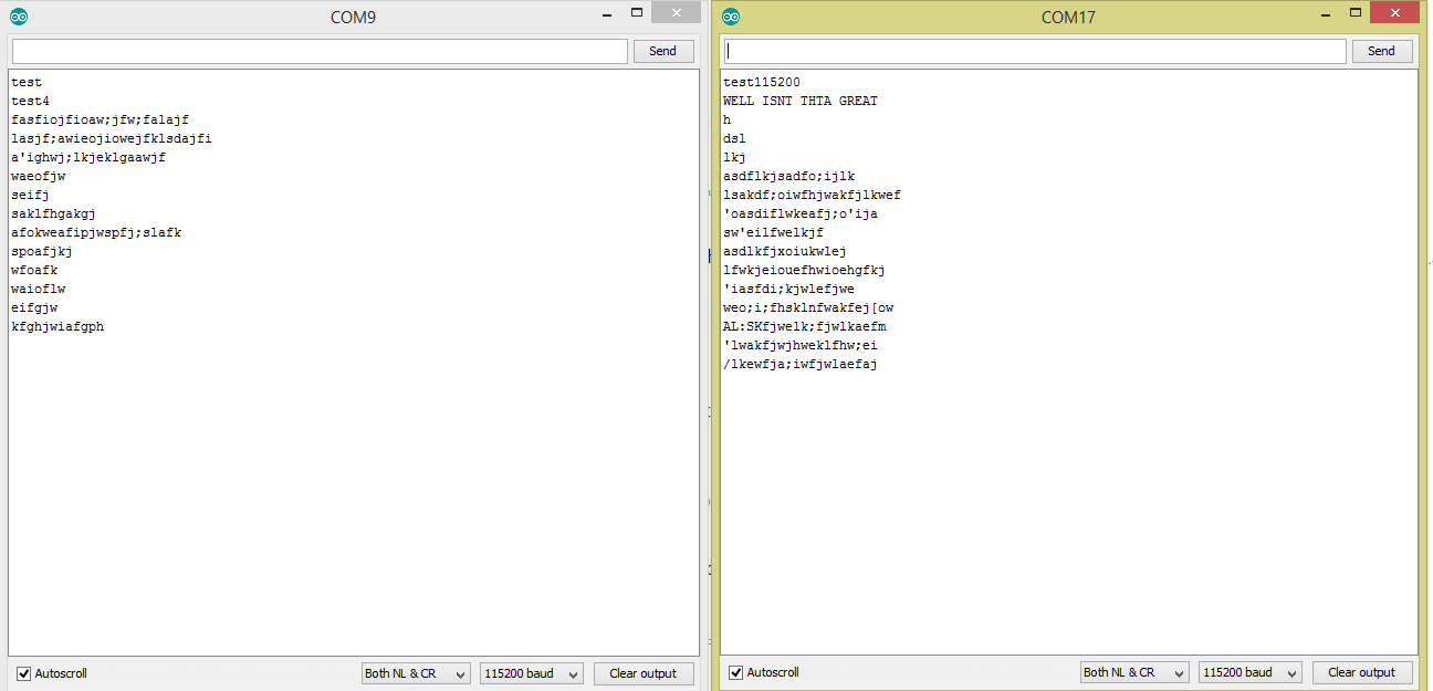
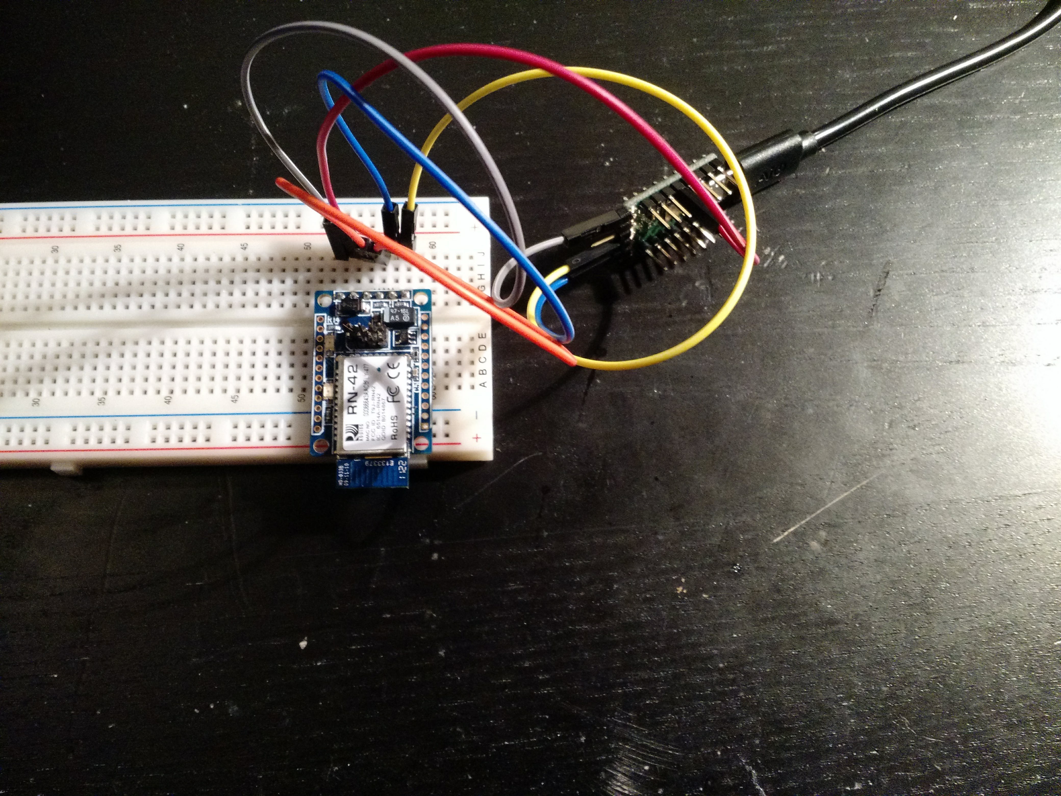
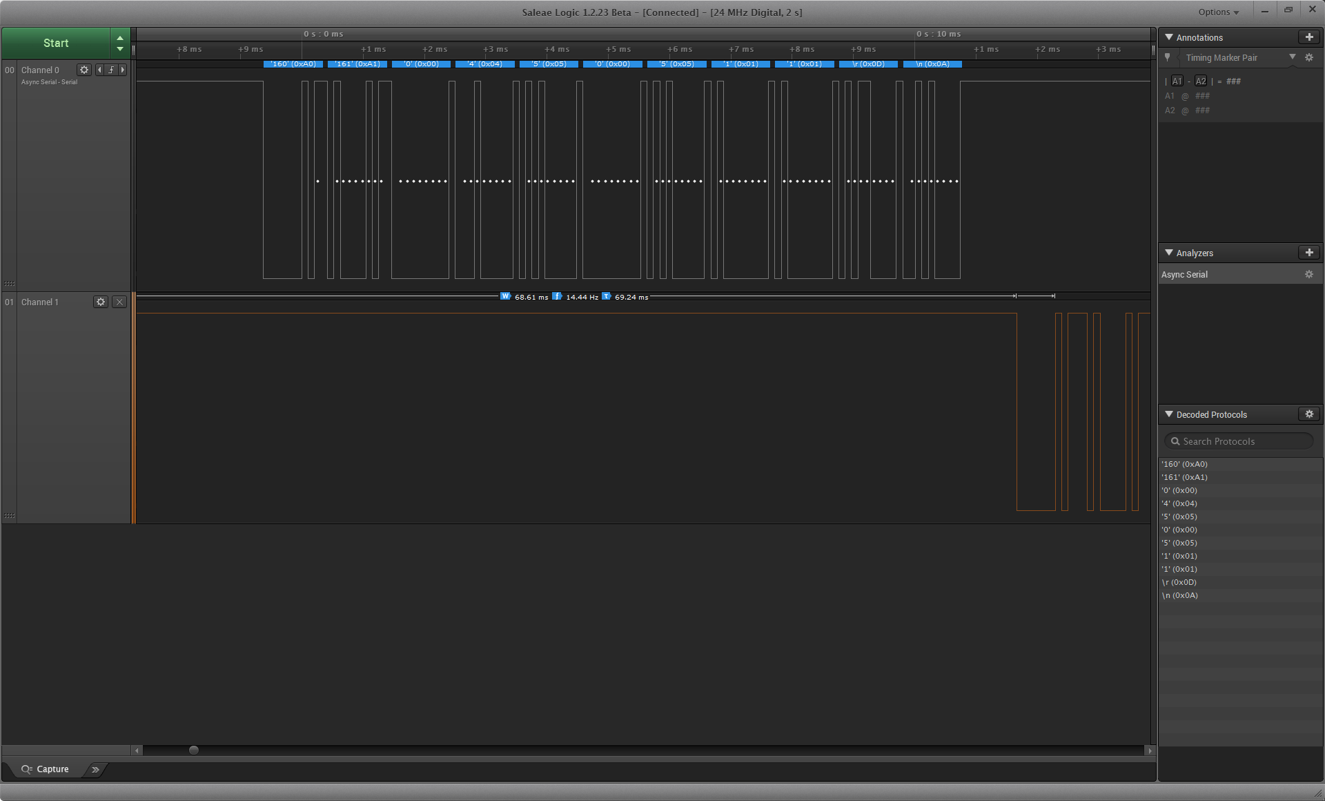
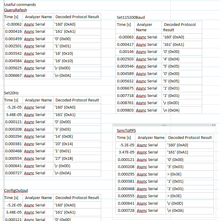
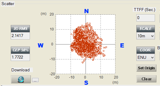
    I’m still not sure what the issue was but everything seems to be working now. I’m able to send configuration messages and have them change parameters. Now that the problem is behind me I can start digging into the workings of the module.

    For use in MagiLog there are a few settings that we’ll need to set. We need to set the update rate to 20Hz, align the messages to UTC seconds, and increase the baud rate. App note AN0003 covers the binary format used to communicate with the Venus modules.

    This is the overall structure of the message, it’s fairly straightforward and won’t be too difficult to work with. One thing to note is that each message needs a checksum number generated to be sent with the message. Since there’s only a small number of messages I’ll ever need to send it will be faster for me to just extract the messages with my Logic and export the values from the software.

    Once I had everything configured how I wanted I set up the antenna and let it sit for a few hours. Here are the results I got.

    As you can see the overall spread is sizeable. That said, the calculated accuracy is actually better than what is advertised, 1.77m vs 2.5m. This was in less than ideal conditions, so I’m impressed. By combining the GPS data with the accelerometer data, I think I can get that error down even more.

    The last feature that’s worth covering is the 1 pulse-per-second (1PPS) output. It’s accurate to around 20ns and will be stable throughout a wide temperature range. I’m looking into using it as a reference for the other trigger clocks to keep all the data aligned. From what I can tell it should work and will make a lot of timing issues much simpler.

View all 22 project logs

Enjoy this project?

Share

Discussions

Nelson Phillips wrote 04/04/2018 at 13:08 point

Hey, interesting project. See you might be using air pressure sensor for it. Been playing around with some for prototyping and have a project about then if you interested.

 https://hackaday.io/project/108157-pneumatic-tech-for-prototyping

  Are you sure? yes | no

Nigel wrote 04/04/2018 at 21:36 point

Thanks for the like. Looking forward to see what you discover.

  Are you sure? yes | no

Similar Projects

Does this project spark your interest?

Become a member to follow this project and never miss any updates