Configuration of the FM receiver was very straight forward. Here is the script in Teraterm language, my preferred choice of terminal software.
; power up the FM receiver: CTS and GPO2 enabled, external RCLK, analog output
sendln '[0x22 0x01 0xc0 0x05]'#13
pause 1
; Get version information
sendln '[0x22 0x10][0x23 r:8]'#13
pause 1
;set FM tune frequency to 8990 = 0x231E
sendln '[0x22 0x20 0x00 0x23 0x1E]'#13
pause 1
;Use GET_INT_STATUS (command 0x14) or hardware interrupts Until STC bit is set
sendln '[0x22 0x14][0x23 r:2]'#13
pause 1
;Call FM_TUNE_STATUS With INTACK bit set (command 0x22)
sendln '[0x22 0x22 0x01]'#13
pause 1
To be added: scope plot of the line out signal and description of listening to it.
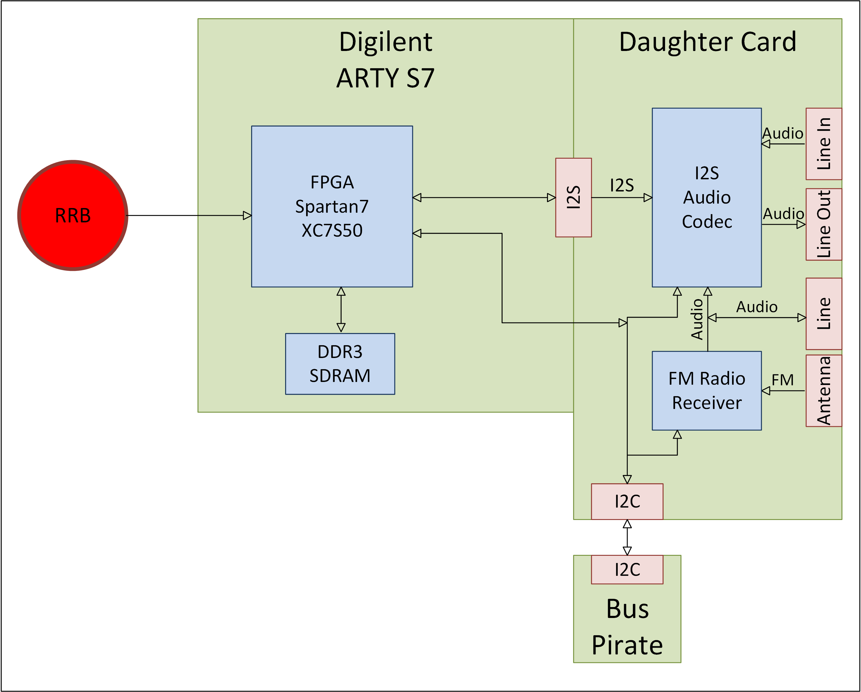
The GPO1 signal on the Si4731 FM chip connected to the ARTY board is held low during RESET. To enable I2C configuration for the chip, it needs to be pulled high by the internal pull-up resistor (weak). A quick cut of the trace fixed this.
The PCM3070 datasheet has unclear information about the REF signal. A schematic has it connected to 3.3V, the pin description states on a capacitor connected for noise suppression. Of course I picked the wrong one and connected it to 3.3V. This fix was a little bit tricky because it was connected to 3.3V between the pin and the cap by a via to a bottom layer trace. But drilling out the via barrel and leaving the track around it intact fixed this as well.
For ease of configuration I am hooking up a Bus Pirate (or as I prefer to call him Bus Privateer, because they are the good pirates) to the I2C interface and run scripts with all config commands through my terminal program of choice (Teraterm).
Example (might be good to put this into the instructions section):
Initial commands:
Bus Pirate configuration and run macro (1) to scan all device:
PCBs are ordered, so are the parts. Boards will be purple and this log will be the collector for assembly and bringing up the hardware. Looking forward soldering the QFN32 0.5mm pitch IC.
Update 13. Aug: Parts are here from Digikey. Boards are in manufacturing.
Update 14. Aug: PCBs are shipped from OSH Park. This is getting exciting (happens every time when FR4 is on the way).
Update 17. Aug: PCBs came in yesterday, beautiful as always. Thanks @oshpark .
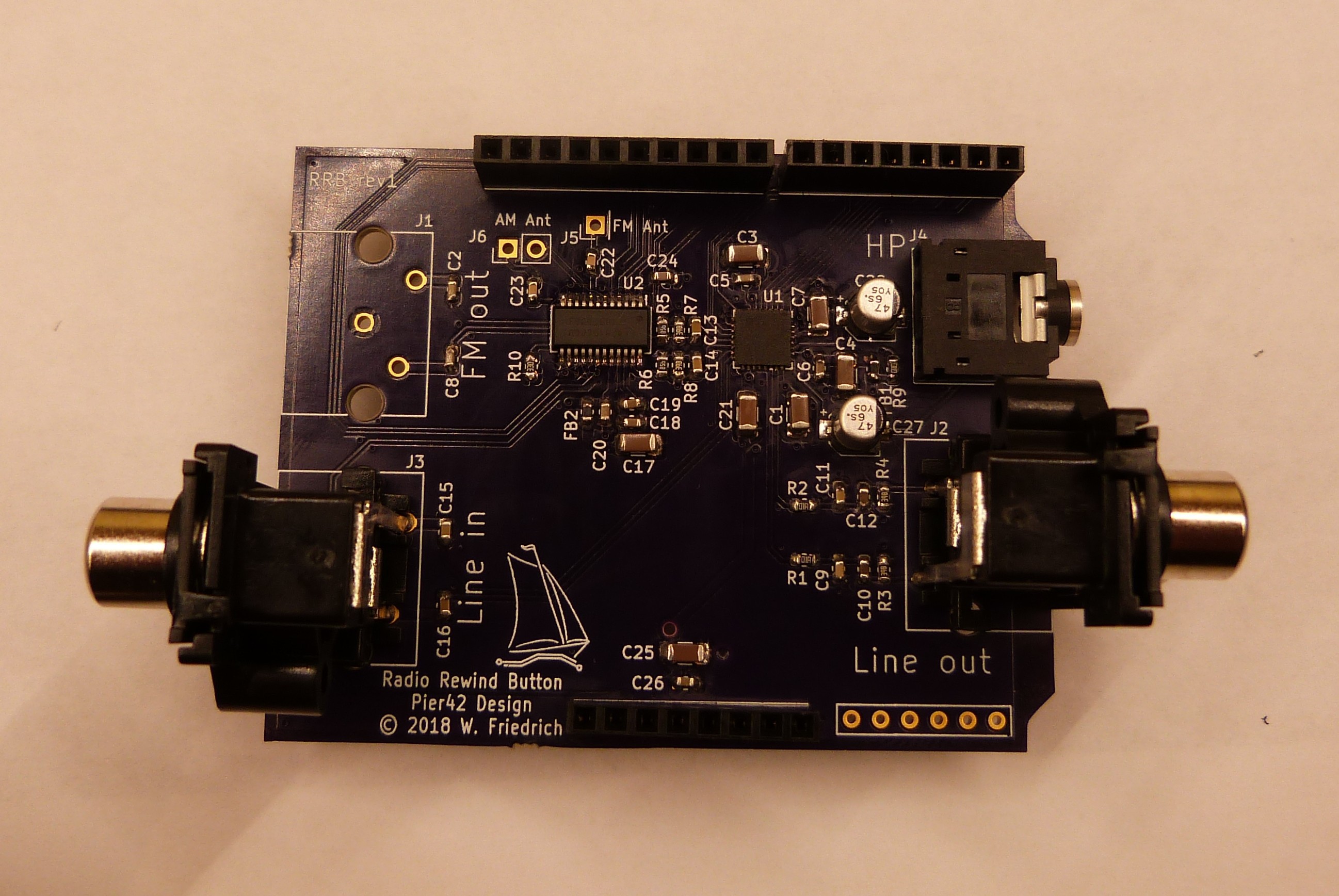
Now the fun part starts with hand soldering QFN32 0.5mm pitch. :))
This was a piece of cake and this is how it looks like:
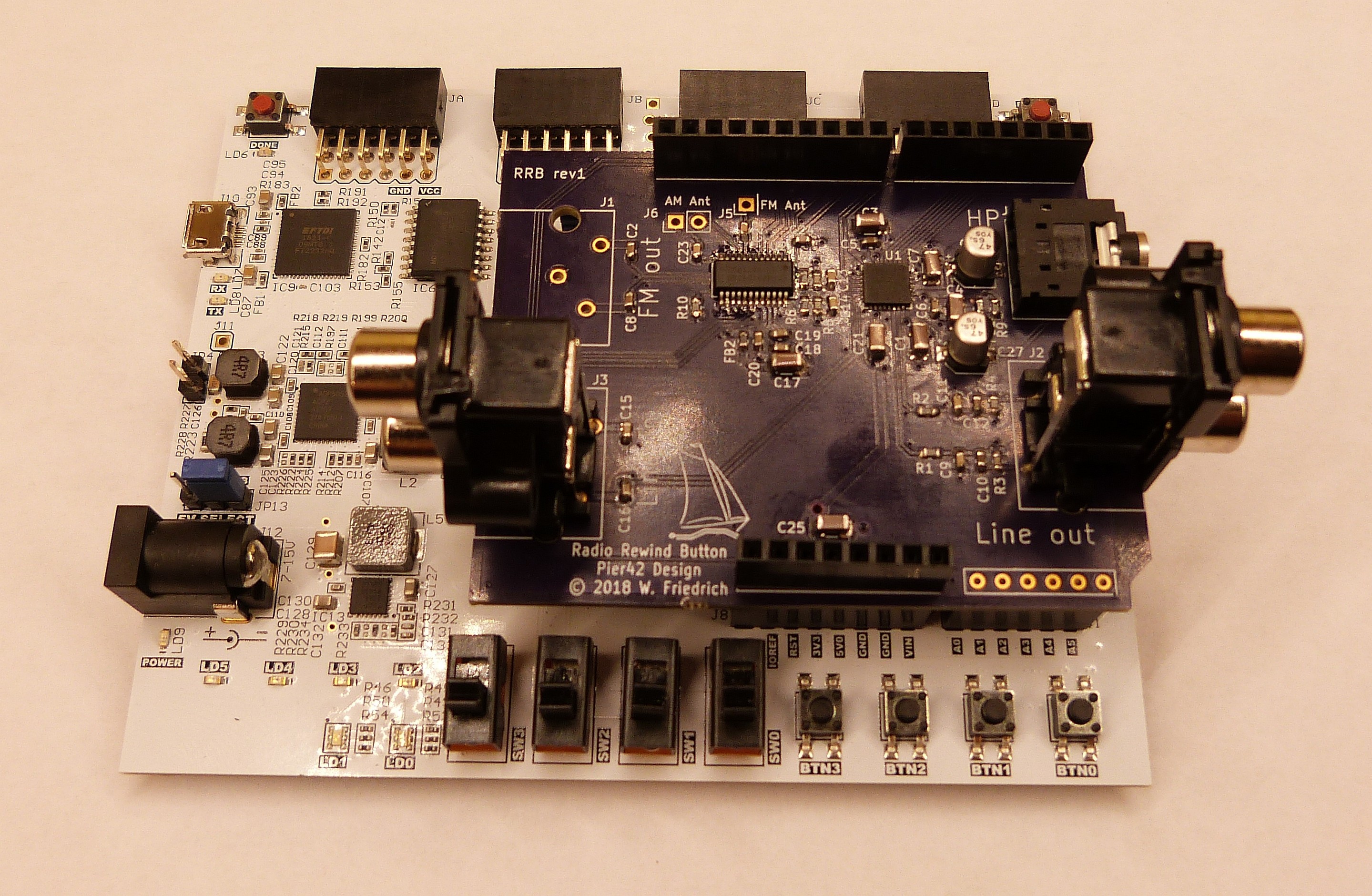
And plugged into the ARTY-S7 board.
Also, I have established I2C communication to the PCM3070 audio processor and the Si4731 FM receiver through the trusted bus pirate.
I just scored a DIGILENT ARTY S7 FPGA board, which is the perfect platform for the RRB project. It has a Spartan7 XC7S50 FPGA and best of all, 256MB DDR3 SDRAM on board already. So I don't have to run a SDRAM interface over PMOD connectors, which was risky from the beginning. And it has Arduino compatible (3.3V) headers. Now I can design a shield with all my crazy audio hardware. All block diagrams will be updated in the near future. Good times.
Just found out that the NXP UDA1380 is end of life:-(. Looks like I am back to component hunting again. Looking for a Audio line in to I2S and I2S to line out codec.
As a replacement, the TI PCM3002 looks very promising. Simple IO but good audio characteristics. I will do some more datasheet reading, but so far it does everything I need. Analog in and out and a digital audio interface, everything controlled through a weird 3-wire interface.Another option would be the TI PCM3070 audio codec chip, which has 3 audio input pairs. This would change the architecture quite a bit, running the FM radio audio stream analog into the PCM3070 and only have a single I2S interface for all digital audio data. Also the control interface is I2C which would help in my quest to save signal pins between the ElbertV2 and my RRB daughter card. Decisions, decisions.
Assuming CD quality, I have 44100 samples/sec in 16 bit. For stereo this is 176400 Bytes/sec or 10584000 Bytes/minute. The smallest SDRAM with availability and second source is 64Mbit x 8 = 67108864 Bytes. So I will have about 6 Minutes and 20 seconds (in NA units this is 6 1/3 minutes ;-) time warp rewind time. This should be more than enough to listen to the missed news and not many songs are longer than 6 minutes, unless your really like November Rain or Pink Floyd and have a radio station that plays the songs to the very end and not only half </rant>.
Heart of the prototype will be a Numato Elbert V2 FPGA board. It has a Xilinx Spartan3 XC3S50A FPGA, which is somewhat unfortunate for me as a lifelong Altera guy but they all speak VHDL.
It should be large enough to handle a SDRAM core and 3 I2S interfaces. The board has 39 dedicated IOs and I am sure the 6 LEDs and 8 DIP switches can be re-purposed if necessary. The buttons might come in handy for a user interface, except the big red button of course, which will be there no matter what. 32 IOs are located on 4 PMOD connectors. the daughter card will connect through them and will mainly hold the SDRAM interface (~30GPIOs for a 64M x 8bit device). 64Mx8 is the smallest I could find with an 8bit data bus to save pins and available quantities. Also on the daughter card will be the FM radio and the line in and out interfaces. Separate control interfaces will go to an Arduino controller, could be as simple as an I2C interface. The prototype might connect to a PC for user IO, but the end goal is a small display showing the radio station and other useful data. The big red button was part of a Sparkfun dumpster dive shipment, waiting patiently for its opportunity to shine.
 MagicWolfi
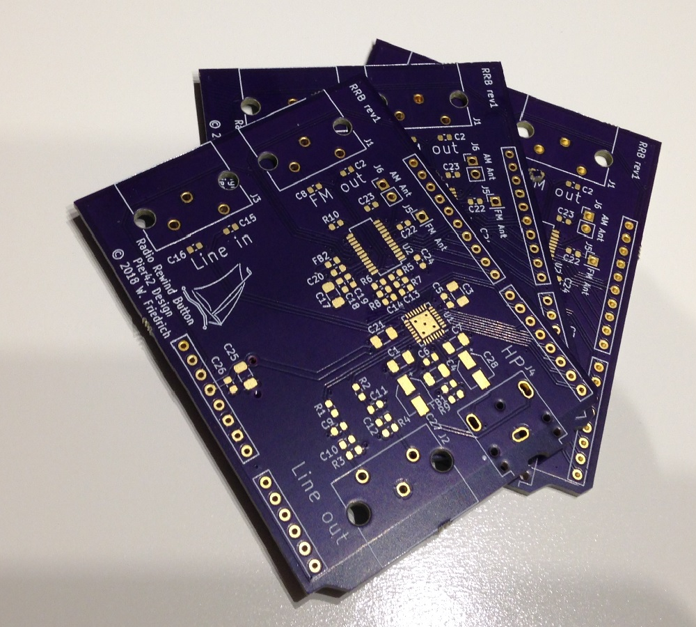
 Another option would be the TI PCM3070 audio codec chip, which has 3 audio input pairs. This would change the architecture quite a bit, running the FM radio audio stream analog into the PCM3070 and only have a single I2S interface for all digital audio data. Also the control interface is I2C which would help in my quest to save signal pins between the ElbertV2 and my RRB daughter card.
  Decisions, decisions.