-
The real hardware runs Apple 1 Basic !
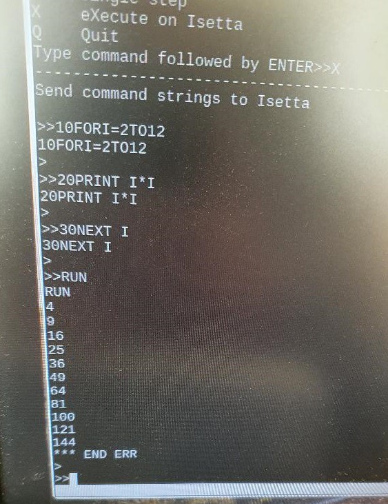
04/19/2024 at 19:07 • 0 commentsA major milestone was reached today ! The original Apple 1 BASIC, programmed by WOZ, is running on the real Isetta hardware ! It runs on the intended 12.5 MHz (80nS cycle time).
For character I/O, there is a synchronous serial link with a Raspberry Pi. The screen and the keyboard of the Raspberry Pi are used to communicate with Isetta.
Here you see a screenshot of the RPi screen. After the ">>" (generated by the RPi) the RPi reads a full input line, echoing it on the screen. Then, after a CR (return), the line of characters is sent to Isetta Apple Basic, and Basic again echoes the characters to the screen. Then the output of the Basic interpreter follows, and the Basic prompt ">". Note that there is an "*** END ERR" because there is no END statement at the end of the program.
PROGRAMMER
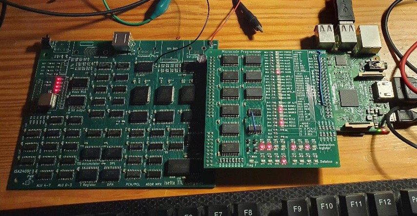
Quite some work had to be done after the prototype was soldered. I had to make a Python program on the Raspberry Pi to program the microcode into the three microcode flash chips. On the programmer board (described in the previous log) a small change was needed. This Python software can also execute arbitrary microcode on Isetta, and run a test program that tests hardware functions.
The programmer can grab the clock of Isetta, by putting the first 74AC163 clock divider into LOAD mode, and providing a new clock (SW generated by RPi) to the first two preset inputs of the 163. The transistor that transferred this clock was, unsurprisingly, not fast while switching OFF, and I suspected that was the reason that I sometimes got a bad working instruction during singlestepping. This transistor also did the 3.3V to 5V translation. I replaced it by a simple diode with a 1N5 cap in parallel. It's a poor man's level converter. At the high RPi 3V3 level, 0.7 V is added by the diode so the ac163 sees around 4V on its input. That worked, errors now occurred rarely, and could be handled by a retry mechanism in the programmer.
How does the application program (the 4K Basic interpreter) get into the main RAM ? I could modify the programmer such that it writes to RAM instead of microcode flash. But I already had a mechanism in place that would also work with a fully stand-alone power-on and reset. A certain part of the microcode copies the BASIC interpreter program from the microcode flash to the main RAM, soon after reset.
![]()
COMMUNICATION
Next thing was communication (characters in, characters out) between RPi and Isetta. It should also work when Isetta generates VGA output, so we are handling a single bit directly after the horizontal interrupt. (That is generated by a simple hardware timer).
The bit handling should always take exactly the same amount of cycles, independent of the data send or received, otherwise there will be jitter in the generated VGA output.When the VGA output and keyboard are working, we still need this interface to the RPi to transfer files to or from Isetta. We could also use the RPi screen as debugging output while an application runs on the VGA screen.
Since it should also be possible that a PS/2 keyboard is connected to Isetta, the choice was made to use the same receiver hardware and software for the keyboard as well as for data coming from the Raspberry Pi. Since it uses open collector outputs, both clock and data signals can simply be tied together. This combination was not foreseen when the PCB's were designed, so a few wires had to be added.
Communication RX receive driver
The keyboard has two lines, KB_CLK and KB_DATA. Both lines are driven by a open collector output on a standard PS/2 keyboard (pullup resistors in Isetta). If no information is sent, both lines are high. The keyboard receive driver will be able to receive scancodes that are sent by the keyboard. It has the following states:
- Wait for startbit. If the clock line has a falling edge, and the KB_DATA line is low, the startbit is valid and we proceed to the next state. If the data line is high at this falling clock edge, we stay in this state.
- Read databit. There are 8 of these states. If the clock line has a falling edge, the data line will be sampled and its value will be shifted into the keyboard-read register. Bit 7 in this register will be the bit that was sent first. This will be repeated 8 times. After that, we will continue to the parity-bit state.
- Read parity bit. If the clock line has a falling edge, the data will be read but it's value will not be used. But the value of the keyboard-register will be transferred to the keyboard buffer. The keyboard buffer can contain 255 values. There is no check if it is full. (Assumption is that the SW works faster than I can type).
- Read stopbit: This is not implemented. It's function will be done by Wait-for-startbit.
The keyboard-receive system will also be used to transfer information from the Rasberry Pi to Isetta. The microcode programmer pcb has two open collector outputs for this purpose, that are (on Isetta) directly connected to the two wires coming from the keyboard. On the RPi this uses GPIO27 and GPIO2.
So, with a simple program on the RPi, the RPi keyboard can be used for Isetta. Instead of scancodes, ASCII codes will be sent over the connection. In the future, this ASCII encoding might be slighty changed, so that it does not overlap with scancodes, and Isetta can see if the info comes from a PS/2 keyboard or from the RPi.Note that a PS/2 keyboard sends the LSB first, while the above receive system stores the first received bit in
the MSB (used because it gives simpler microcode). So Isetta receives reversed scancodes.Communication TX transmit driver
The same keyboard driver will also handle traffic in the other direction (This is NOT the system that is used to send information to a PS/2 keyboard ). This uses a third wire called GP_OUT1, that is an output for Isetta and an input for the RPi. It is called GP_OUT1 because it can be used for other purposes when this TX function is not used.
The output is synchronous, clocked by the KB_CLK signal that is generated by the RPi. It requires that the RPi sends a keyboard byte in order to receive the TX information. The RPi must send a low startbit, and if there is no key to send, the databits should be all ones so Isetta sees a FF character and can dismiss it. Sending FF also provides a good synchronisation on the startbit.
In Isetta, data to transmit must be put into the transmit buffer. It can hold 255 characters.
The keyboard states have the following functions for TX:- Wait for startbit. If the clock line has a falling edge, and the KB_DATA line is low, the startbit is valid and we proceed to the next state. If the data line is high at this falling clock edge, we stay in this state. The tx-register is loaded from the transmit buffer, but if the transmit buffer is empty, the tx-register is set to FF. The empty/non_empty state will be remembered in a tx_state register. So, if there is no data to send to the RPi, the RPi will receive a FF byte.
- Read databit. There are 8 of these states. If the clock line has a falling edge, the tx-register will be shifted left, and the bit that is shifted out will be put on the GP_OUT1 line. This will be repeated 8 times. After that, we will continue to the parity-bit state.
- Read parity bit. If the clock line has a falling edge, it will, if tx_state is 0, increment the pointer to the transmit buffer.
- Read stopbit: This is not implemented. It's function will be done by Wait-for-startbit.
In each line interrupt, this RX+TX code will take approx. 16 cycles.
Changes to Apple Basic
Apple Basic uses memory locations for its character I/O. In Isetta, the 8080/Z80 IN/OUT instructions
will be used for I/O. These IN/OUT instructions were also added to the instruction set of the 6502 (with exactly the
same opcode as on the 8080/Z80, possible because 6502 has many unused opcodes).At this moment, port 0x31 is used for RPi/KB input as well as output. But 0x31 is not yet set in stone.
- IN 0x31 ; Reads KB scancode or input from RPi. Returns byte in ACC. When no byte available, returns ACC=0 with Z_flag=1.
- OUT 0x31 ; Writes character in ACC to RPi, and when the buffer is full, returns ACC=0 with Z_flag=1.
addr = 0xe3d5;  // address where bytes must be changed in output routine

memory[addr++] = 0xD3; // OUT (opcode 0xD3)
memory[addr++] = 0x31; // port 0x31
memory[addr++] = 0xF0; // BEQ  (try again if buffer was full)
memory[addr++] = 0xFC; // -4
memory[addr++] = 0x60; // RTS


addr = 0xe003;  // address where bytes must be changed in input routine

memory[addr++] = 0xDB; // IN (opcode 0xDB) new keyboard-input instruction
memory[addr++] = 0x31; // port nr
memory[addr++] = 0xF0; // BEQ, loop while buffer is empty
memory[addr++] = 0xFC; // -4
memory[addr++] = 0x09; // ORA #80
memory[addr++] = 0x80; //
memory[addr++] = 0x60; // RTS,  char in acc.
A lot more to do, a few things:
- Getting VGA output to work
- Make a simple file system in the 32Mb serial flash
- Get PS/2 keyboard working
I bought a PS/2 keyboard online for about 20 Euro, but it keeps sending the same data at fixed intervals. A little online searching learned that my keyboard model only works after it receives a reset command. So that will be a small hardware and software change to add transmitting a reset message to the keyboard.
Supporting a PS/2 Mouse would also be nice...
-
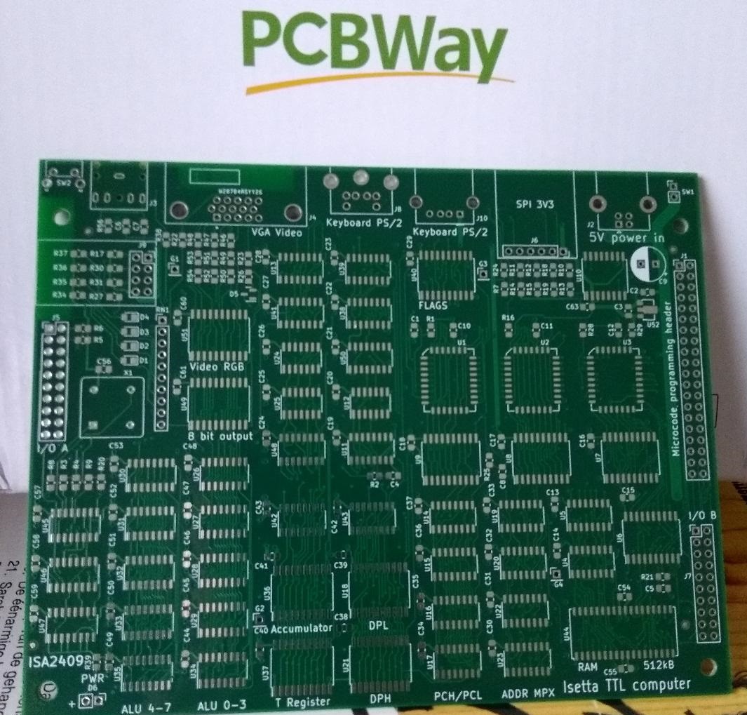
PCB and parts arrived !
03/11/2024 at 14:16 • 0 commentsI received the PCB's ! These PCB's were sponsored by the kind people of PCBWAY. As always, they are of a very good quality.
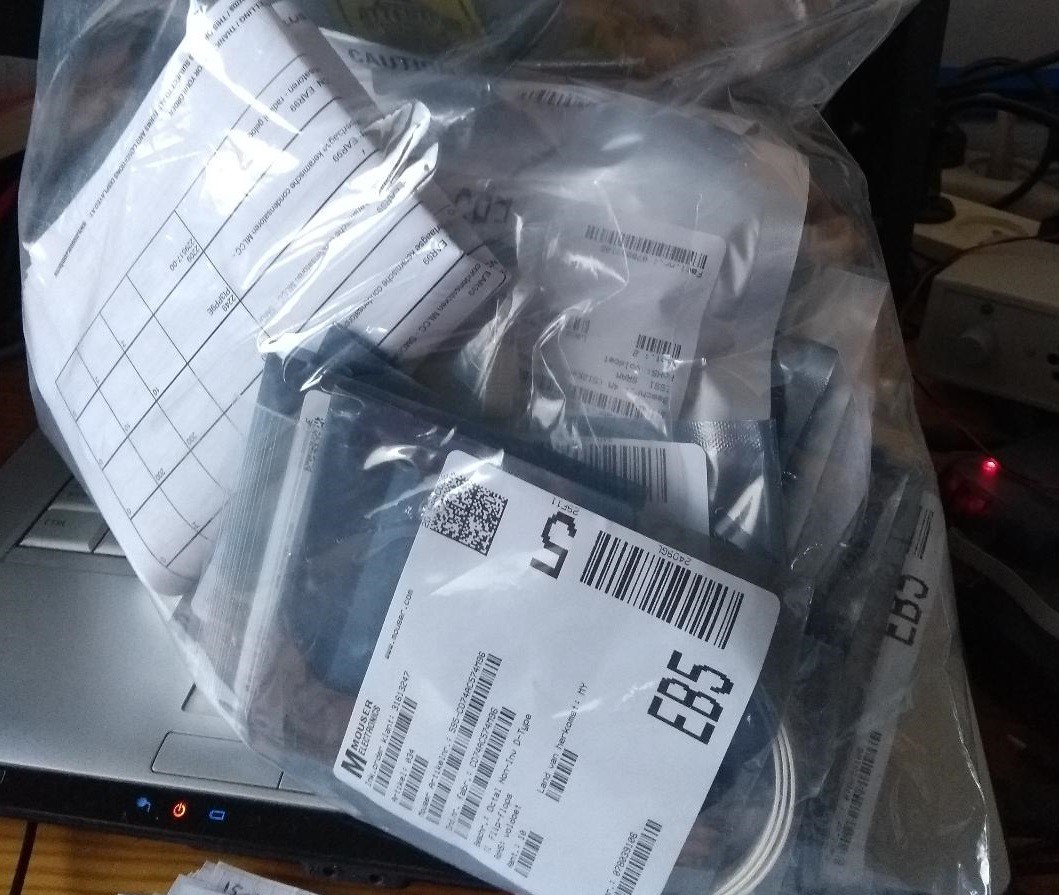
And I also received a big bag of parts:
![]()
Warm up the soldering iron !
-
PCB finished, Logisim simulation, and programmer
02/22/2024 at 20:25 • 0 commentsLOGISIM simulator
The design was only tested on the logical level, in the Javascript simulator. Before making a PCB I wanted some form of confirmation more on the hardware level, so I entered the design in the good old Logisim.
Nowadays there is a further developed version, called Logisim Evolution. I tried it by loading one of my old designs in it. It became a big mess with long hex-sequences appended to my net names, and many shapes not displaying correctly. And indeed, Evolution is no longer compatible with the old file format. That's a pity, because I had quite a lot TTL devices converted to Logisim circuits.
So I stayed with the old version, 2.7.1, so I could use my library of TTL components. And I found a few mistakes in my design. Also found a way to save a chip on the generation of the horizontal sync pulse.
But it is slow. At it's top speed (Logisim says it is 4100 cycles/sec), when you type a short line of Apple Basic, you have to wait one minute before the prompt reappears !
PCB Finished
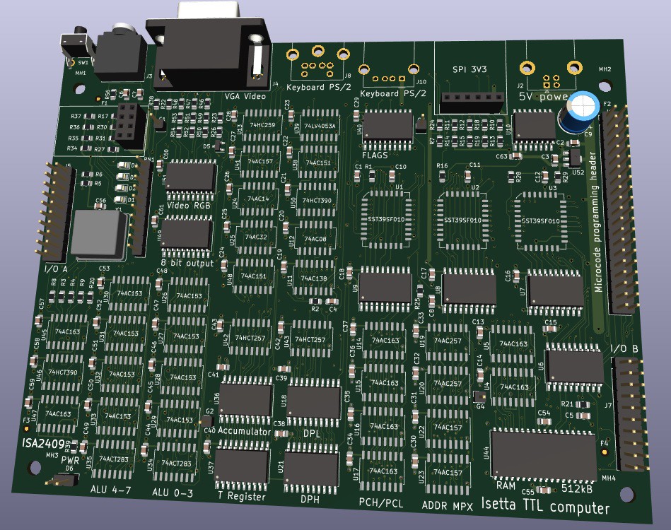
I finished PCB design. Here is the nice 3D preview of KiCad:
![]()
It is 119 x 150 mm (4.7 x 5.9 inch), 4 layers.
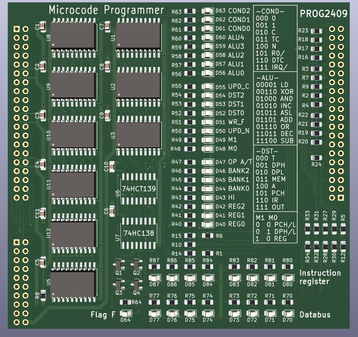
Microcode Programmer
I also needed a programming interface. Previous projects used the Raspberry Pi for that. The Pi has enough GPIO pins to accommodate the 8 or 16 bit wide Flash memories of those projects. The interface was not much more than a small universal board, with resistors for 5-to-3.3 volt conversion.
But in the Isetta the microcode flash memory is 24 bits wide. That is almost all I/O that the Pi has, not leaving enough for control signals. So now I use 8 bits I/O from the Pi. The data going to Isetta is first transferred to three HCT574-type registers (the HCT will also translate 3.3V to 5V), and then it can be transferred as one 24 bit value to Isetta. For data going to the Pi, there are three LVC244 chips to convert 5V to 3.3V. Only one of the LC244 is enabled to transfer its value to the Pi. There are two more LVC244, one for the databus and one for control signals from Isetta to the Pi.
The new RPi programmer is only required once, to program the microcode. The program for the 6502 or Z80 can reside in RAM, and can be programmed in BASIC or any other convenient language.
The Raspberry Pi has the following control outputs to Isetta:
- Disable the data output of the 3 Flash chips
- Give a programming pulse to the 3 Flash chips
- Take control of the Isetta CPU clock signal
- When it has control, send a clock to the Isetta CPU (to single-step it).
The RPi also has a few serial lines to/from Isetta, intended for character read/write so you can use the RPi as a terminal as long as Isetta has its video and keyboard interface not yet working.
Here is how it looks. Isetta connects to the left side, and the RPi to the right side. It also has LED's for the 24 microcode signals (with explanation on the pcb), and LED's for the databus and the instruction register. The LED's will also work if the RPi is not connected. It is a 2-layer board.
![]()
-
PCB design progress
02/14/2024 at 14:22 • 0 commentsHere is the current state of the design, it's almost finished. The Flash chips had to change from DIL to PLCC, because the required 55nS speed is not available in DIL.
![]()
-
Re-started PCB design, in SMD
01/28/2024 at 09:20 • 0 commentsSince I last worked on the PCB design, there have been many changes.
And after looking at the availability of the chips, I found that several of them were not in stock (in DIL version). And since the design has become faster, it is not as easy any more to switch between the TTL logic families, because for many chips, the speed is critical.
This made me decide to switch to SMD devices. Only the microcode flash chips will stay in DIL, so they can be easily taken out to program them (although there will be a system to program them while they stay on the board).
Here is a preview of the new design:
![]()
Dimensions are 12 x 15 cm ( 4.7 x 5.9 inch). It will be a 4-layer board. It is designed to fit in a Hammond RM2055S enclosure.
-
Less parts and higher speed
12/04/2023 at 20:36 • 0 commentsIt's been a while since I wrote a log. In this log I will tell you what happened to the design in the past months.
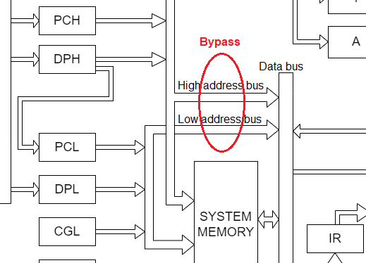
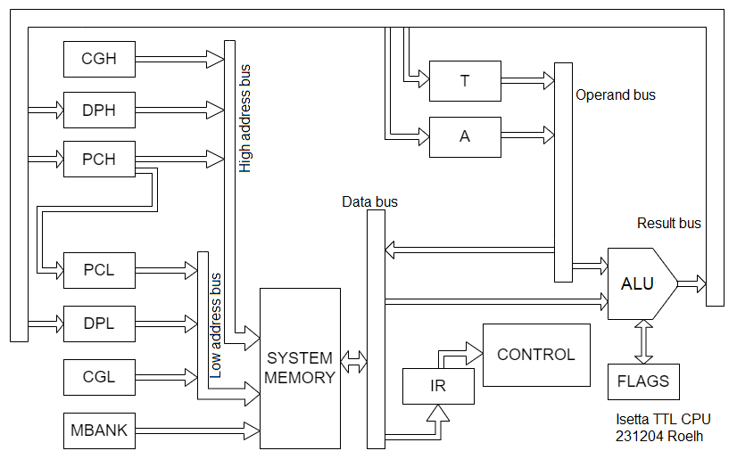
BYPASS
The design has a few buffers that implement the "bypass". This can place the address registers on the databus, so we can inc/dec them, or store them to T and then to memory. This is also the path to store the program counter (pch/pcl) for a CALL instruction. And it is used to add the offset to the PC in case of a branch.
![]()
As always, I was looking for components to remove, to get a low-component-count design. And indeed, we can do without the buffer for the low address bus ! We can simply put a 1-to-1 table in a zero page of memory, and an access to this table will give us the register value on the databus. The high address bus must be 0 to access this table, that it is already an existing function.
We have 8 memory banks, so there is a maximum of 8 zero pages, enough space in zero page. One of the zero pages already has a table for right-shift.
For the high byte, this is less useful, since the table would be scattered through memory, occupying one byte in every page. That is not a good idea.
But... the only register that we need from the high bus is PCH. And the PCL bus is not loaded from the result bus, but from the DPH register (in this picture, that is. It was later changed to come from the T register).
If we modify it, and load the PCL register from the PCH register, we can access the PCH contents by loading it into PCL first ! In fact, when we write a new value to PCH we will at the same time (with the same signal) write the old PCH contents to PCL.
![]()
For doing a jump, first write the LSB to PCH, and then write the MSB to PCH (that will move the LSB from PCH to PCL). And for a CALL, first save the PCL address through the 1-to-1 table, via the ALU, to T. T is then stored to the stack. After the LSB of the subroutine address has been written to PCH, the old PCH is in PCL and can now also be saved to stack.
The control signal for the bypass is obviously no longer needed. Used it later to double the amount of RAM-based registers.
The 1-to-1 table in RAM is built by microcode, directly after reset, in the same loop that fills the right-shift table.
Changes for this were done in the simulator and the microcode generator.
SPEED
In october I did some timing calculations, using the typical values for 74AC logic. (These typical values are only in Fairchild datasheets, not in the Texas Instruments datasheets).
I was a bit surprised to see, that with some measures, the clock speed could be doubled to 12.5 MHz !
We would need a 10nS RAM. Circuits in the address bus needed a few changes to make it faster. One of the address signals (for the CGL register) came from a 74HC238 1-to-8 decoder that had a quite big delay. It was used to extend the number of memory-based registers. This way of extending the number of registers was dropped (replaced by a directly available microcode control bit). This HC238 also delivered a signal to select SUB and a signal to select DEC in the ALU. This could be changed to a single signal for both SUB and DEC. Other functions in the HC238 could also be solved in a different way. The HC238 could be removed.
The circuits for the flags had to change, in the design the CY-out of the adder sometimes had to pass four devices before a flag result could be clocked-in in its register. The flag system was changed such that the adder-cy-out is used at only a few places. The condition-selector can choose it, and in a group-1 instruction it can be put into the C flag. The adder-cy-out now only has to pass 2 devices. The last of these is a 74HC4053 analog switch, that is slow in switching to the other channel, but relatively fast to pass a signal. Since the switch channel can be setup at the start of the cycle, it is expected to be fast enough.
The adder-cy-out signal is called TC (temporary carry) in the microcode. For group 1 instructions, this signal is stored in a register, to make this signal accessible to later microcode instructions, this register output is called DTC (delayed temporary carry). This signal DTC can now also be chosen by the condition selector (after shuffling some of its inputs).
Today I uploaded a new schematic to the file section, that also mentions the timing of the relevant signals. The critical path takes a calculated 74 nS, so that will be fast enough for the new 80 nS cycle time.
Changes were needed in the simulator and the microcode.
There were several other changes, too many to mention them all.
-
Colors
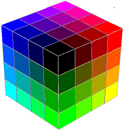
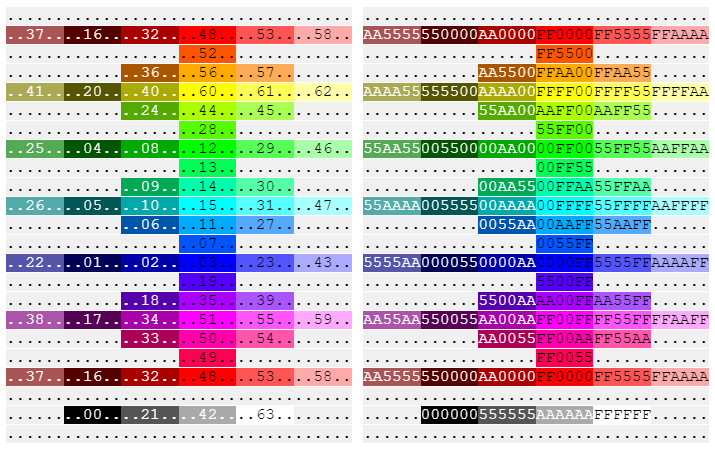
08/24/2023 at 18:34 • 1 commentThis computer will have 64 colors (2bits red, 2 bits green, 2 bits blue).
I was curious what the colors would look like, so I made a kind of three-dimensional plot with dimensions red, green and blue. It became a cube, built from 64 small bricks. If we look at the cube with the black brick pointing to us, we see this:
![]()
So, starting from the black brick going to the right, we see increase in the red component. To the left, we see increase in blue component, and from black going down we see increase in green component. At the circumference we see the bright rainbow colors, and the remaining colors are darker versions of the colors.
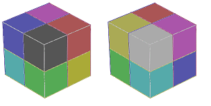
At the opposite side of the cube (unvisible in the above picture), we have a point where the amount of all primary colors is maximal. That is the color white. If we look at the other side of the cube we see this:
![]()
At the circumference we see the same bright rainbow colors again. The remaining bricks are the lighter versions of the rainbow colors.
But we did not see everything ! At the inside of the cube, there are 8 bricks that we didn't see yet. These are light-grey, dark-grey, and a grayish version of the primary colors:
![]()
So here we see the eight hidden bricks, shown from both sides.
The following table shows these colors, numbered from 0 to 63, and also with their hexadecimal web color. The first column has the grayish colors, and black, white and the two greys are at the bottom:
![]()
So this table will be a help if I ever come so far to program colored stuff for my contraption.
-
Video system
08/22/2023 at 18:51 • 0 commentsThe Isetta video system will now be described.
GENERAL
The generated signal is a VGA signal with a maximum resolution of 640 x 480 pixels.
The timing is:
25.175 master clock
approx. 40nS per pixel (for 640 pixels/line)
approx. 32uS scanline
A whole scanline has a width of 800 pixels (only 640 pixels used)
A whole frame has a height of 525 scanlines (480 scanlines used).
Exact values can be found here.The isetta can work with maximum or reduced horizontal resolutions:
- 40nS per pixel (for 640 pixels per line)
- 80nS per pixel (for 320 pixels per line)
- 160nS per pixel (for 160 pixels per line)
In the vertical direction, scanlines can be repeated (to keep the pixels almost square, also when a lower horizontal resolution is used), giving:
- 480 lines, or
- 240 lines (480 divided by 2), or
- 120 lines (480 divided by 4)
There are 64 colors (but the color can not be freely chosen for every pixel).
HARDWARE PRINCIPLE
The Isetta processor runs with a cycle of 160nS (6.25 MHz). The video output is directly generated by the processor, so during every instruction, one or more pixels must be generated:
- 1 pixel/instruction (for 160 pixels per line)
- 2 pixels/instruction (for 320 pixels per line)
- 4 pixels/instruction (for 680 pixels per line)
Isetta contains a hardware timer that triggers an interrupt at the beginning of every scanline. At the beginning of the visual part of the screen, this interrupt transfers control to the microcode that has the video instructions to give screen output. It can also initiate the generation of the frame sync pulse (the line sync pulse is generated by the hardware timer). If the interrupt is outside the visible area, the interrupt code will only increment the line counter, and return to the interrupted program almost immediately.
A video instruction will get a single byte from the RAM, and gets color information, pixel information, and sometimes control information (flags) from that byte.
The microinstruction fetches this byte from the indicated RAM location.
The RAM is normally addressed with the (PC++) mode (Of course this requires that the PC that was used in the Z80 or 6502 program was saved when the interrupt is entered).The color information is 6 bits. The instruction can store the color in register T (foreground color) or in register A (background color).
Information about a pixel is only 1 bit. If that bit is 1, the color of the pixel comes from register A. If the bit is 0, the color comes from register T.
We now come to the basic byte formats that are used for the video system.
- Color definition:
Byte format: -cccccc-
The 6 color bits 'cccccc' can be transferred to the T (Foreground, FG) or A (Background, BG) register.
- 320 pixels/line :
Byte format: a------b
Two pixel bits 'ab' select the two pixels to be used in 320 pixels/line mode. These pixels are placed in the 4-bit 'pixel register' as 'bbaa'. The pixel register is loaded at every instruction, so the information is only available in the next cycle.
- 160 pixels/line :
This format is the same as the 320 pixels/line format, but in this case the bits a and b simply have the same value.
- 640 pixels/line :
Byte format for 4 pixels: --pppp--
Four pixel bits 'pppp' select four pixels to be used in the 640 pixels/line mode. These pixels are transferred to the DPH register, and the output of this register is connected to a multiplexer that selects the correct pixel to be displayed. The 'pppp' bits are in bit5, bit4, bit3 and bit2 of the byte. The pixel register is connected to other inputs of the same multiplexer.Byte format for 2 pixels: ab-----1
This 2-pixel byte must be loaded with a SHL (shift left) instruction, while shifting a '1' into bit0. That will put the bits in the 4-bit pixel register as '11ab'. The '11' section defines background color (in register A).
- Select pixel register or DPH register:
One of the bits in the microinstruction ( ctl_reg1 ) determines if the pixel information comes from the 4-bit pixel register or from the four '--pppp--' values in the DPH register. This is done in the cycle that follows the instruction that loaded the byte.
Note that there can be combinations of bytes:
- Color can be combined with 320 pixels/line, to 'accccccb'
- Color can be combined with 640 pixels/line, to 'abccccc1' (only 5 color bits here)
- For 640 pixels/line, 4 pixel and 2 pixel format can be combined to ab-pppp1 (defining 6 pixels)
APPLICATION OF THE VIDEO INSTRUCTIONS
At the start of the visible area, the processor should set the 'blank' signal (in the output port) to zero. This enables the video output, and selects the A or T register on the operand bus, based upon the pixel value (while this selection is normally determined by the microinstruction). During video output, the microinstruction can select A on the operand bus to force the color to background.
At the start of a video line, a table will be accessed that has the relevant information for this line:
- The start address of the video data. The SW can manipulate this address, e.g. having the next line point to the same data address, for 240 lines or 120 lines mode. The video data address will be placed in the PC.
- A pointer to the video instructions to use, that will determine the actual video mode for this line. So the video mode can be different for each line.
- A default value for the FG and BG color (for 640 pixels/line mode).
- For 40-char text mode, a byte that contains the row address of the character generator.
320-pixel/line Graphic mode
A normal 320-pixel/line can alternate between loading a new FG color and loading a new BG color. Every instruction will also provide the two 'bbaa' bits to the pixel register.
A <- (PC++) // load BG color and ab bits, display 'bbaa' in next cycle
T <- (PC++) // load FG color and ab bits, display 'bbaa' in next cycle
A <- (PC++)
T <- (PC++)
A <- (PC++)
T <- (PC++)
etc
640-pixel/line 2-color graphic mode
A 640-pixel/line can be used for 2-color graphic output. The FG and BG colors must already be present in the A and T registers:
DPH <- (PC++) // provide four --pppp-- bits
DPH <- (PC++) // provide next four --pppp-- bits
DPH <- (PC++) // provide next four --pppp-- bits
DPH <- (PC++) // provide next four --pppp-- bits
etc
40-char/line text mode
The 320-pixel/line graphic mode can also be used to display text.
But it is also possible to use a character definition bitmap somewhere in memory. We spread the definition of a single row (6 pixels) over 3 memory banks. These locations also contain the foreground color of the character.
The first instruction places the character code in DPL. The DPH register is already set to the correct row of the character (done before the start of the line). The video data can be the same for each row in a character. If we start the video data at address 0x0400, the behaviour will be similar to the text mode of the Commodore 64: Write an ASCII value in the range 0x0400-0x7FF and the character will appear on the screen.
dpl <- (pc++)  // char code.  DPH is set at beginning of line. Suppress pixels(with A/T select)
T <- (dph/dpl,bank1)  // pixels/color accccccb  (color specified in bitmap)
T <- (dph/dpl,bank2)  // pixels/color accccccb
T <- (dph/dpl,bank3)  // pixels/color accccccb
etc
2-color 80-char/line text mode
We use essentially the graphic mode for this. The 640 pixel/line mode will probably be used with 400 or 480 lines per screen, so this will take a lot of memory (But we can use a memory bank outside the normal 64kB area).
There is way to reduce the memory usage when text is used, by providing 6 pixels in a byte, in the ab-pppp1 format. A first instruction will load the byte and display the '11ab' bits in the next cycle. The next instruction will display the 'pppp' bits in its next cycle.
So the character is 8 pixels wide, but the first two pixels are '1' (background).
DPH <- (PC++)   // load ab-pppp1 and display 11ab in next cycle
NOP             // display pppp in next cycle
DPH <- (PC++)   // load ab-pppp1 and display 11ab in next cycle
NOP             // display pppp in next cycle
etc
Multicolor 80-char/line text mode
In this mode, the first instruction loads 2 pixels and a 5-bit color. The next instruction loads 4 pixels, together this are 6 pixels for the character. This repeats for the next characters. So every character can have a different color.
T <- shl(pc++)  // abccccc1, 2 pixels, shift, pixels 11ab, color ccccc1
DPH <- (pc++)   //  --pp pp--, load 4 pixels
T <- shl(pc++)
DPH <- (pc++)
etc
[ Edit 230830 The definition of the byte formats, and the application section, have changed. This log was made up-to-date. ]
-
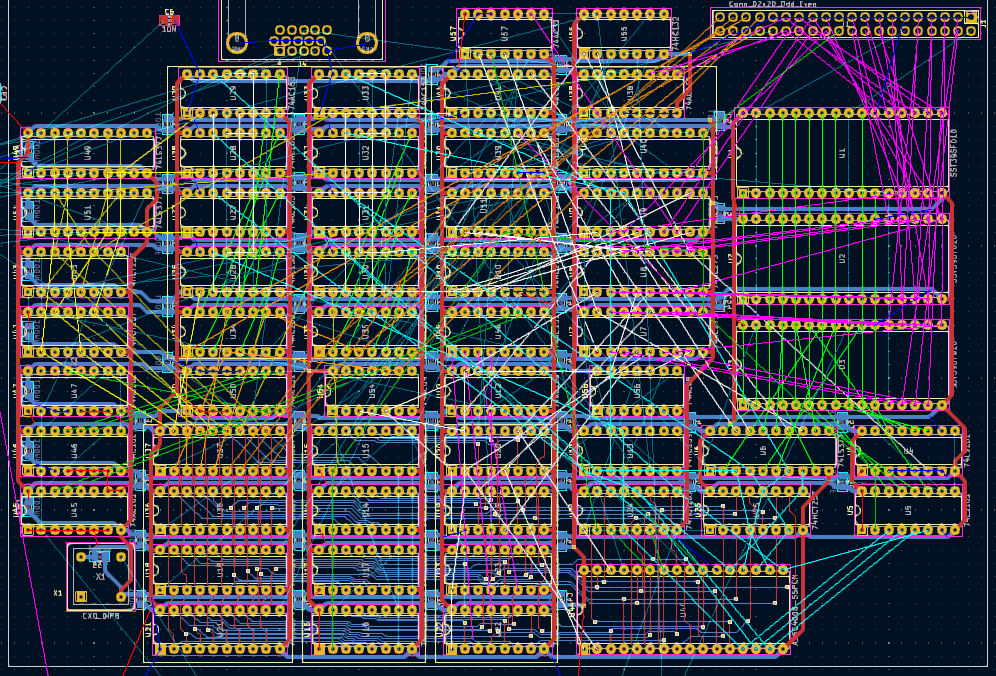
Started KiCad layout
08/06/2023 at 10:49 • 2 commentsThis is the first project where I use KiCad (version 7.0.2).
Schematic entry was quite smooth, but with the pcb layout I experienced some problems. It was difficult to arrange the components on a 0.1" grid. And since I do everything on a 0.1" or 0.05" grid, it is annoying that KiCad displays things like cursor position only in millimeters. [ Edit. You can set this to inches, see comments ].
Routing is not very difficult, but I miss certain functions. But it is possible that I do not yet know all commands for routing.
But don't get me wrong, I think the KiCad developers did a great job !
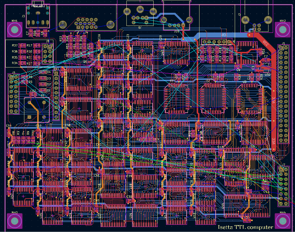
Here is the current state (you can click on the picture to get more detail) :
![]()
The lower part of the pcb is routed. For the rats nest I use several colors:
- red, VCC
- blue, GND
- light blue, databus
- green, address bus, micro-address bus, internal ALU signals
- magenta, microcode bus
- yellow, operand bus
- orange, result bus
- white, several control signals
This is far from finished, especially I/O components must still be added.
-
Update
07/21/2023 at 21:15 • 2 commentsIn the past months i've been working on the hardware design and the microcode.
The number of required IC's got too high in my opinion, so some hardware was removed, every removal costing some effort to implement the removed instruction in microcode. I removed the following items:
- The 74ac151 that calculated the V flag. Now, the two bit-7 adder inputs and the bit-7 adder output, needed to calculate the V flag, are connected to an input port (that has some unused inputs), and the value is saved after every addition/subtraction (or 6502 BIT instruction). When the V flag is tested, it is first calculated (by using the 3 bits to compose an opcode, and executing that opcode).
- The zero-calculation. This was composed of three 3-input NOR gates (74F27) and a 3-input AND gate (74ac11). The other gates in the 74ac11 could not be used somewhere else, so this saves 2 IC's. After a ALU operation, the result byte is now saved to a (memory-based) register called reg_z. When the Z flag is tested (for a BEQ or BNE instruction), an 0xFF value is added to this register (same as decrementing), and when a carry occurs, the value was non-zero. There also was a physical flag Z and a upd_z microcode bit that indicated that this flag had to be updated. Both are not needed any more, and the upd_z frees a microcode bit that will be used to double the amount of available (memory-resident) registers. But it costs one extra cycle at every instruction that updates the Z flag, and one extra cycle when the Z flag is tested.
- The shift-right multiplexers (2 x 74hc157) were removed. Shift-right is now done with a table in RAM (outside normal 64K section). After reset, some microcode constructs this table.
- There was a special 8-bit buffer to put a byte of microcode on the databus. It was intended for special microinstructions that could place this byte in RAM (at an auto-incrementing pc++ position). This would be convenient for moving boot-code to RAM directly after reset. But this can also be done without this buffer, costing one extra microinstruction per transferred byte, and some microcode to organize this.
- It was intended that the video section would have it's own RAM, such that video can be generated while the cpu is doing it's own thing. This will now be an option (additional pcb, called 'performance option' ), and the on-board video is bit-banged by the cpu ( 'economy version' ). It saves around 8 or 9 IC's.
Of course I've been thinking about the video generation. The on-board economy version will have a 6-bit color value in both the A and T register. A multiplexer will select which color is connected to the output. There can be a few video modes, and the video mode can be different for each line. The basic video modes are:
- 160 pixels/line. In every 160nS cycle, the A register will be filled with a new 6-bit color, providing 160 pixels per line, of 64 colors each. (it is just a special case of the 320 pixel/line mode).
- 320 pixels/line. In every 160nS cycle, the A register will get a new 6-bit color. The remaining two bits determine the color of the two 80nS pixels that will be displayed in this cycle. Each pixel is either the foreground color from the A register, or the background color from the T register.
- 80 column text mode. In an 'odd' 160nS cycle, 7 bits will be read, 4 bits will be 40nS pixels in the odd cycle, and 3 bits are 40nS pixels in the next ('even') 160nS cycle. The 4th pixel in this next cycle will be background color (blank pixel between characters). Again, each pixel is either the foreground color from the A register, or the background color from the T register. Since only 7 bits of the byte are used, there is one spare bit that indicates that a new foreground and background color will be loaded in the next two 160nS cycles (while displaying a space character).
During the verical blanking time, the cpu will be executing instructions. At the end of every line, it will get an interrupt, that counts the lines, organizes the vertical sync pulse, and checks if a line of video pixels must be written. (There is a hardware counter that generates the line interrupt).
This week I was working on the interrupt response time. I measured this time with the emulator while running the Apple Basic or TRS80 basic, and the maximum delay between two tests of the interrupt signal was quite long (more than 40 cycles). While most instructions checked the interrupt (by moving the IRQ signal to the F flag, and then jumping to the interrupt routine at the end of an instruction when F is active), there were a few instructions (like conditional jumps) that needed F for another purpose, or that had no opportunity to move the IRQ to the F flag (because moving to F flag does not go together with an ALU operation like ADD, SUB, AND, INC).
The last problem was solved by defining that, at the end of every instruction, the F flag should represent the IRQ state. So the microcode was changed to accomplish this.
The next thing to improve the response time, is to test the interrupt state not only at the end of an instruction, but also in the middle or at the beginning of an instruction (especially for instructions that have a lot of cycles). In this case, a special interrupt entry will be jumped to, that sets the PC one or two bytes back, so the same instruction will be repeated when the interrupt has ended. Of course, the interrupted instruction must not already have done actions that will cause misery when they are repeated.To be continued...
Isetta TTL computer
Retro computer built from TTL, with 6502 and Z80 instruction set. Includes video system.