 Chris
ChrisI'll be honest: sometimes I do a project just for the end result. I know, I know, it's about the journey and the process and the friends you make along the way. I totally get it! But man, sometimes I just realllllyyy want the thing. And it seems like most of the time, the thing is powered by a microcontroller. But I have a simple mind. Much too simple to screw around with wacky custom software and toolchains and to pledge allegiance to some silicon overlord. That's what led me to this project, the CRAPi board.
My two brain cells worked up a storm on this one. I needed the board to be cheap and flexible. I wanted this board to be like ketchup: put that sh*t on everything. That way I could stop thinking about making stuff and actually make stuff. What better sliver of silicon to use for this noble goal than the RP2040? For the price and the PIO capabilities, it fit the bill. That's just the beginning though.
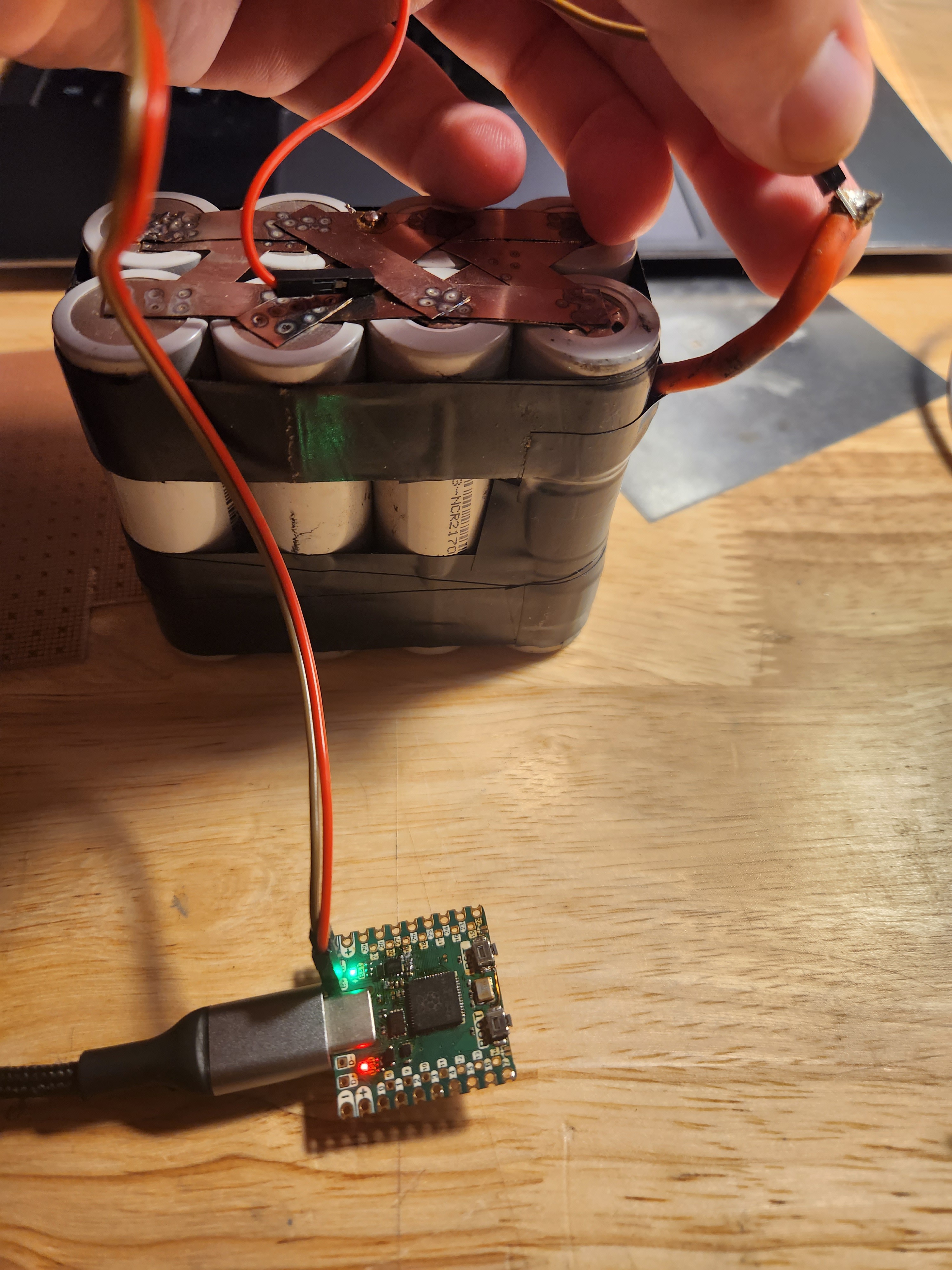
A wise man once told me "Pads are free, dude." And I took those words to heart. How could I squeeze every last bit of usefulness out of the thing that is literally holding the circuit together? Well for one thing, it meant that I didn't need to mess around with a USB-C connector. Upon seeing my substrate only USB-C pads the wise man promptly replied "Well that's a CRAPPY idea." And oh man was he right, that is a crappy idea. But why not try it anyway?
At it's core the CRAPi board is really about being an all purpose dev board without being too flashy about it. What was supposed to be an awful little weekend project to see if you could really make a USB-C connector just out 0.6mm PCB turned into months of purely indulgent feature creep, masochism, and thoughtful design PCB design that borders on unhealthy.
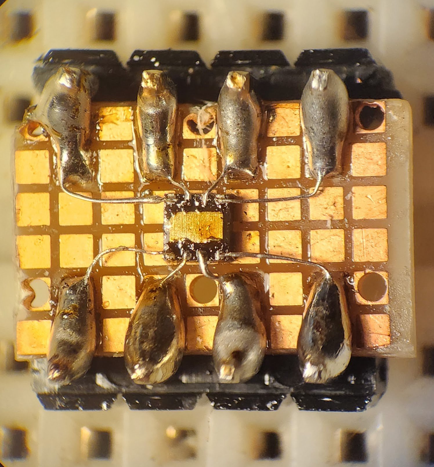
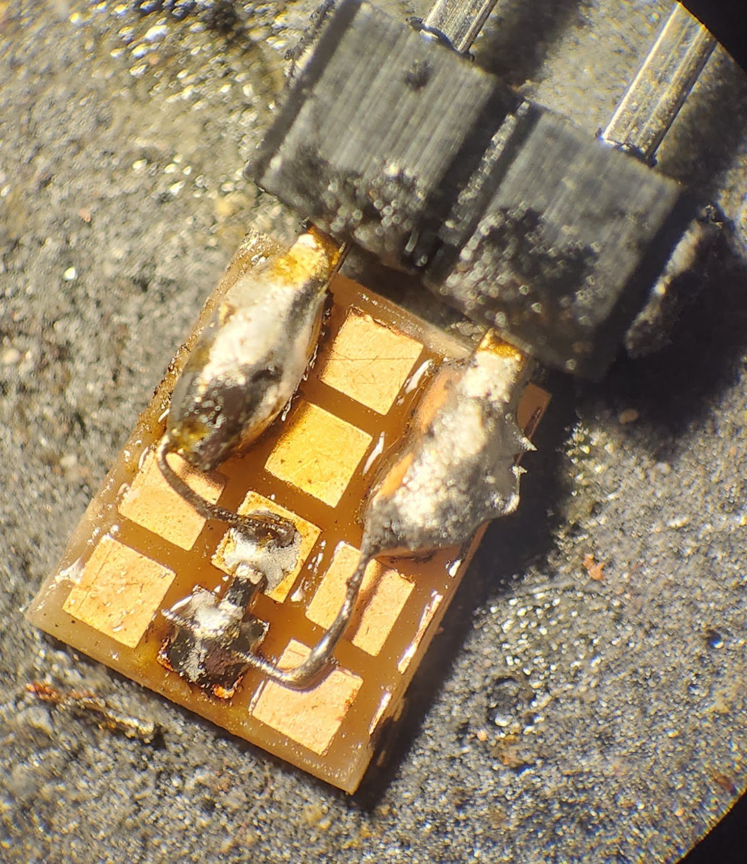
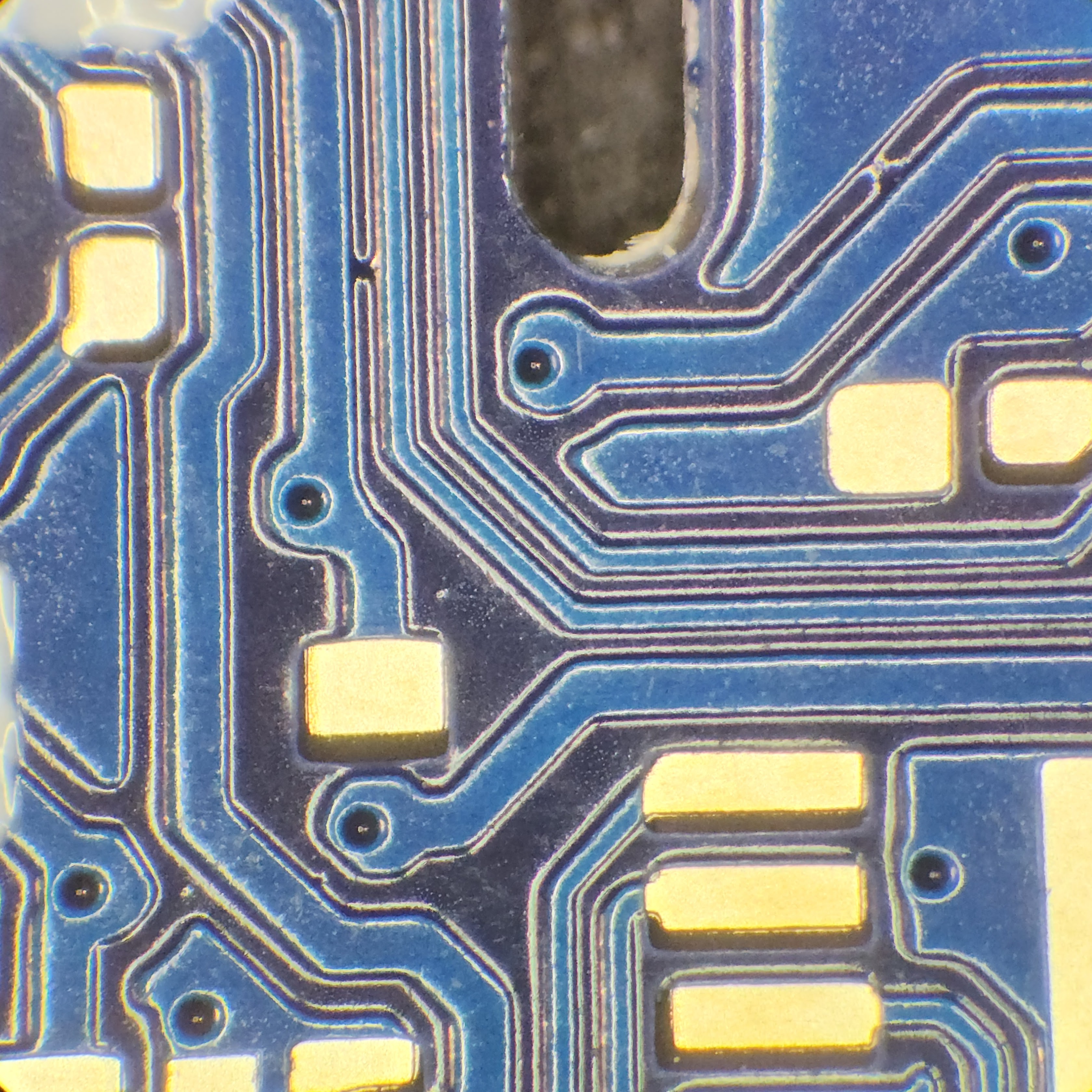
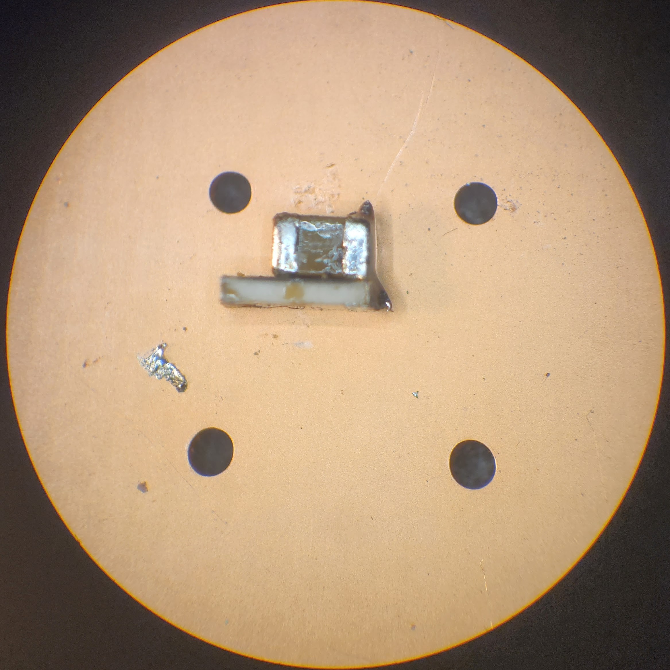


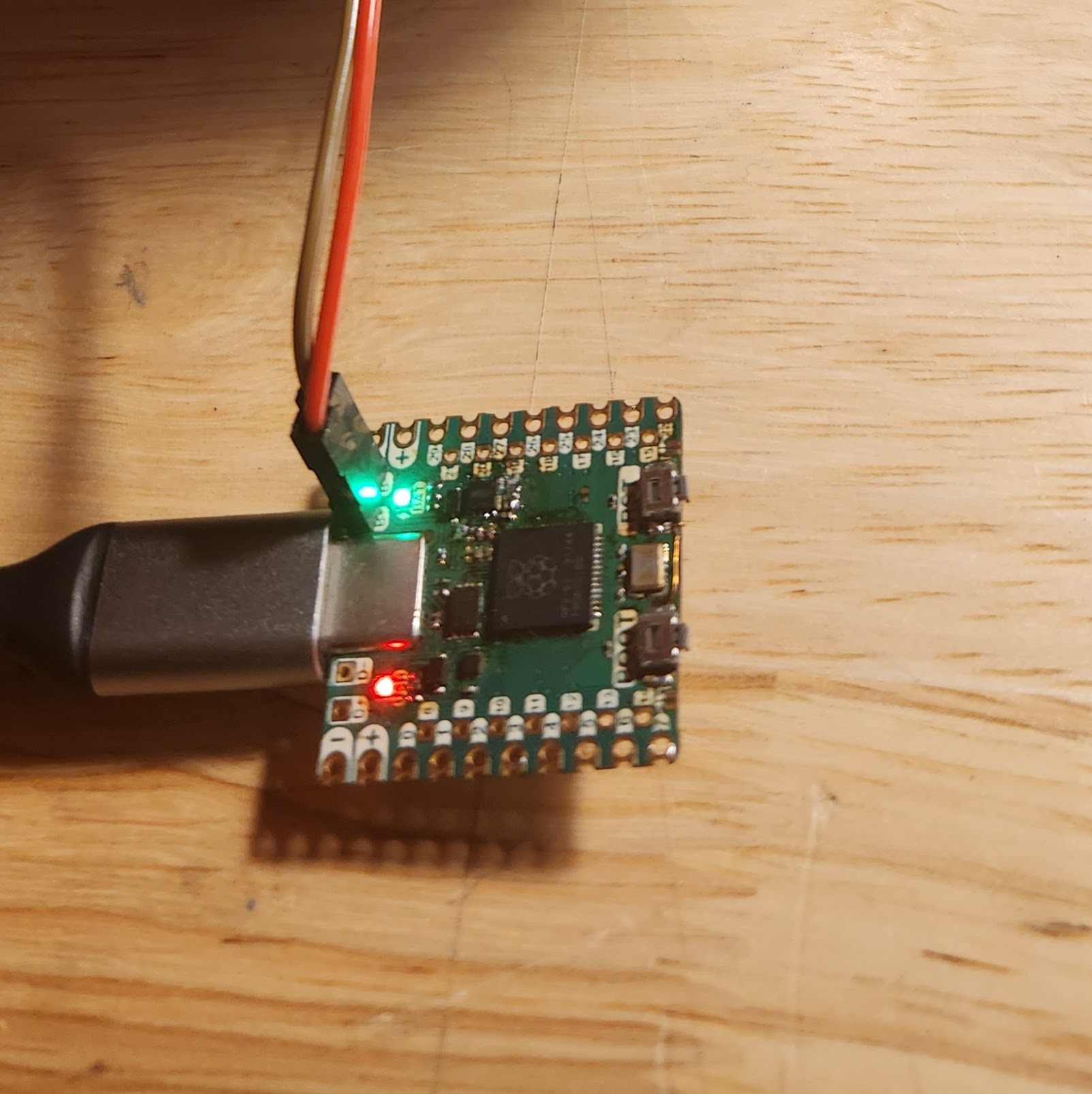
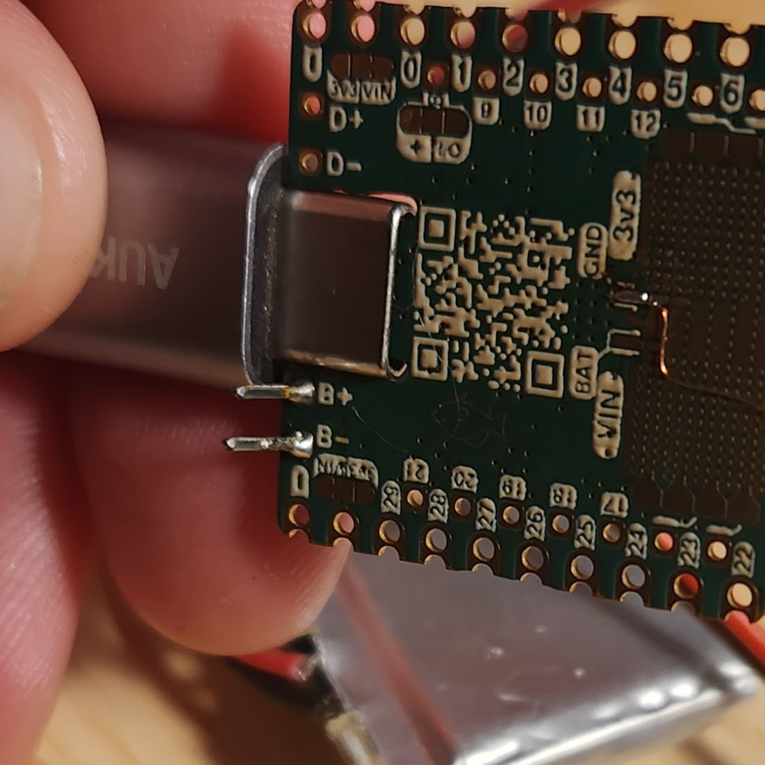
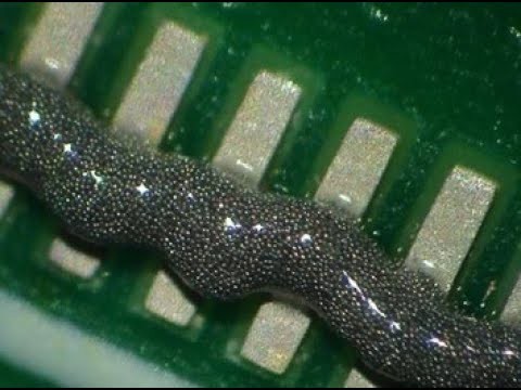
 Again, to my surprise: the footprint worked perfectly. The front anchor tabs of the connector have no problem being soldered down to the GND rail at the bottom of the ProtoGrid. I'm pretty sure I was designing this on a train to Chicago in the middle of the night. So, I don't really remember designing this, but I am glad it worked...
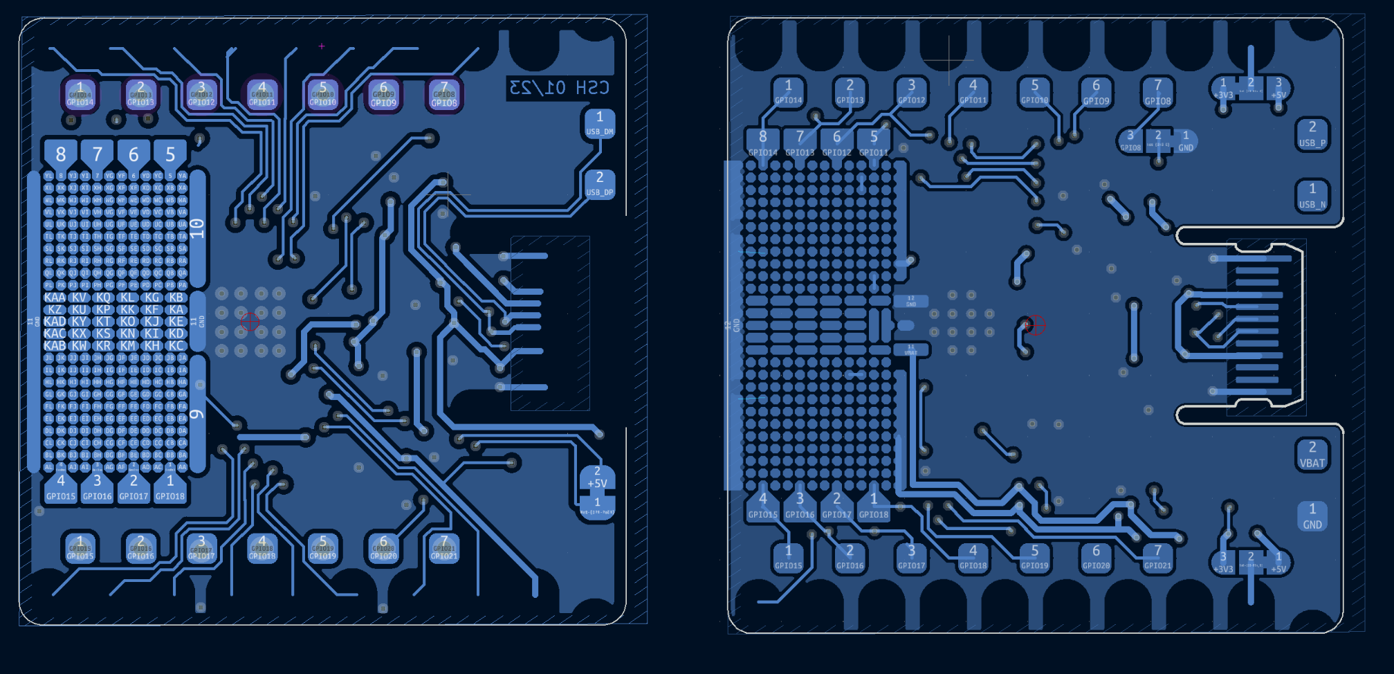 Again, old on the right, new on the left. It gives you a pretty good idea how things changed and why it took 5 months to Rev the board!
  You can also see that I had to give up the mounting hole... I determined that all the new features would be worth give it up. The board doesn't have any components on the back side so you can always double side tape it down. I am also thinking about making some sort of carrier board that would solder to the Thads specifically to add mounting holes. So many ideas so little time.


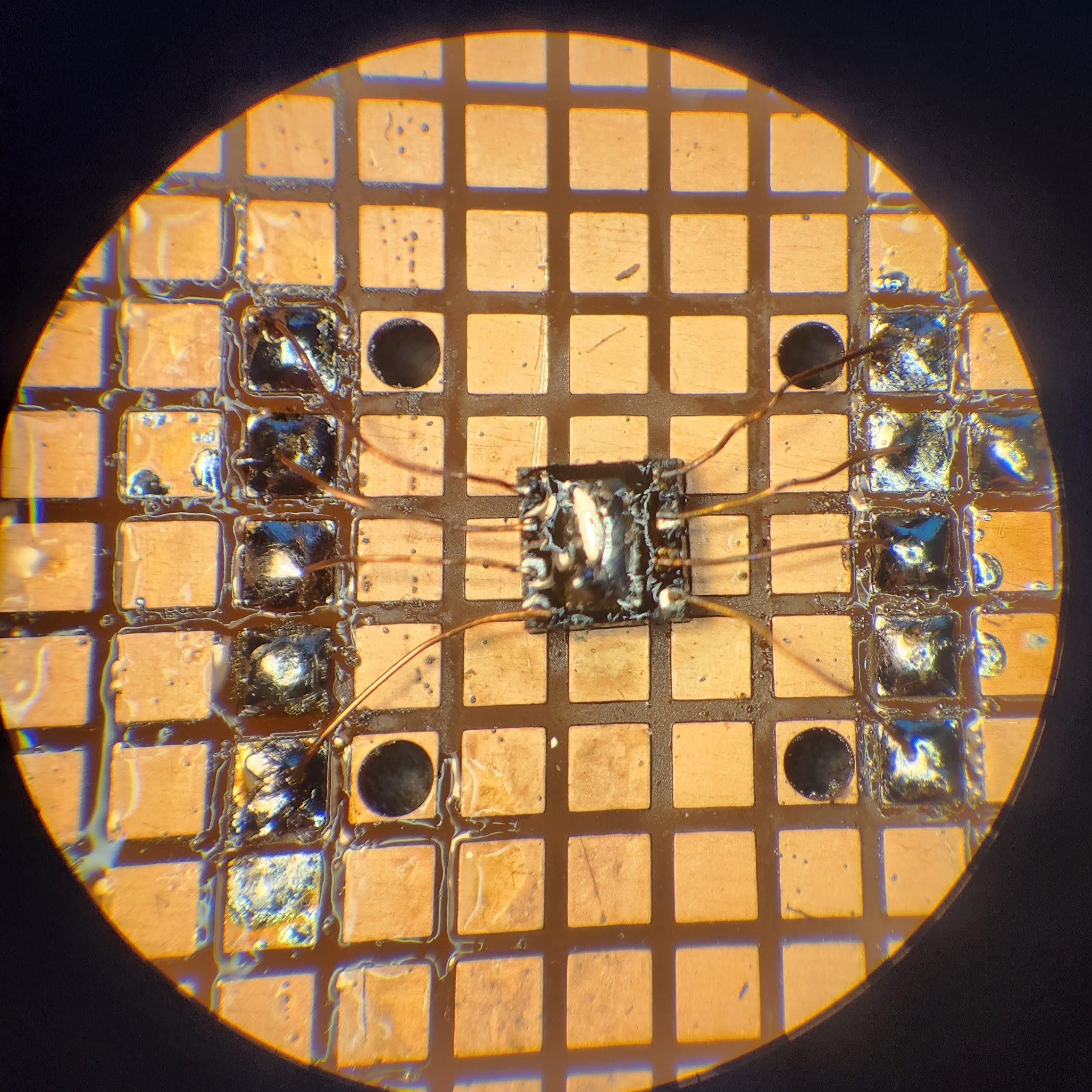
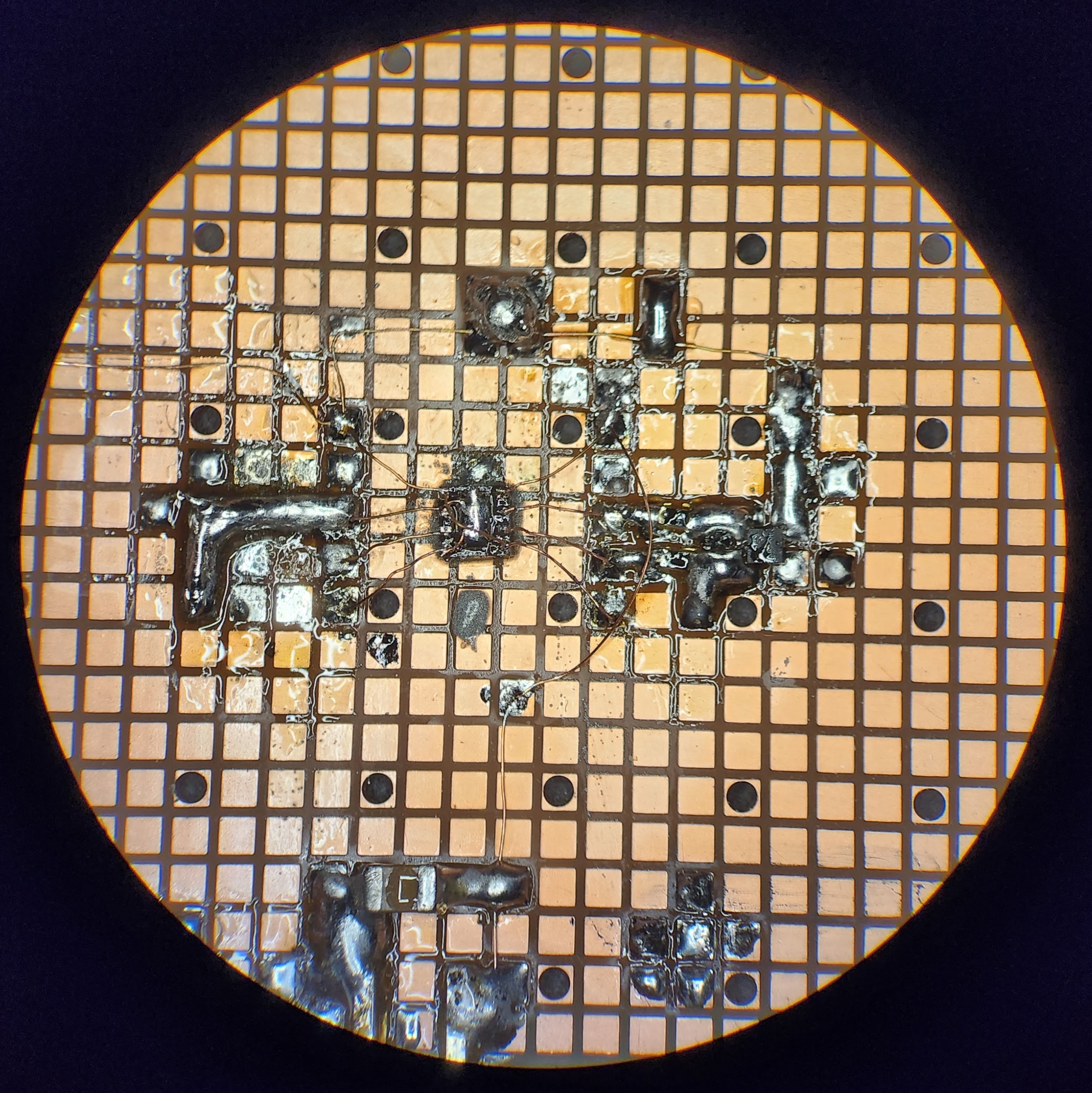
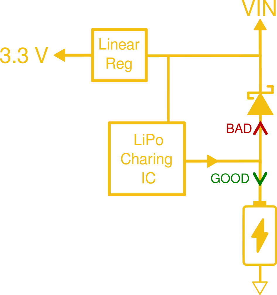
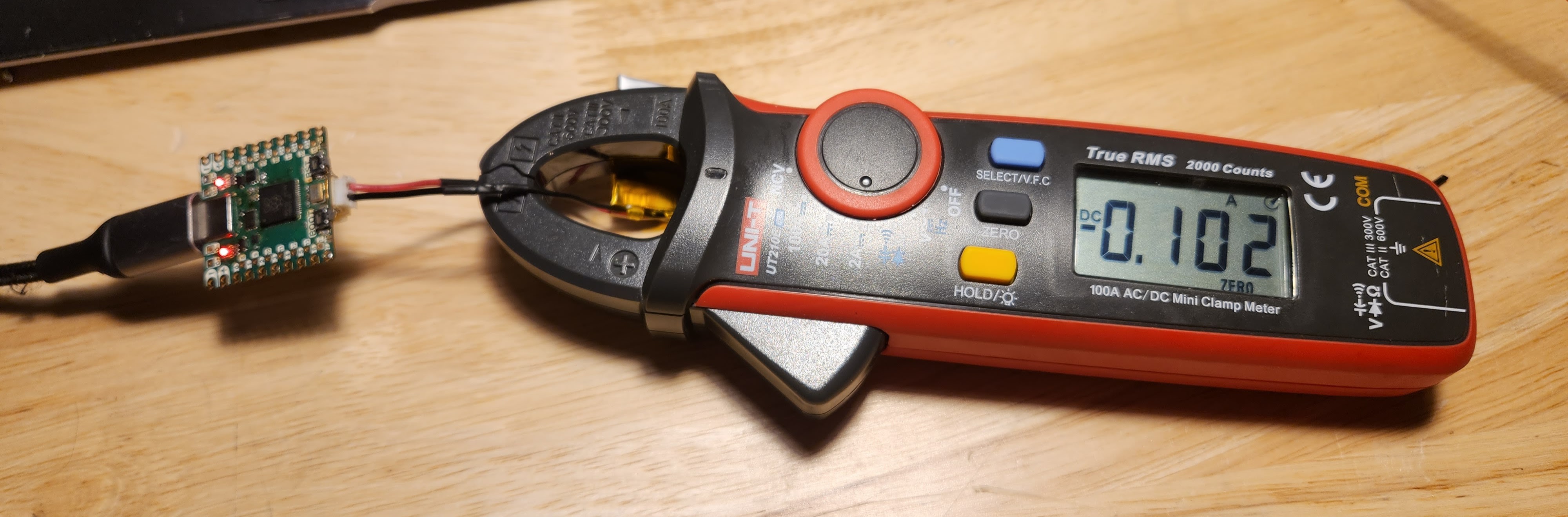
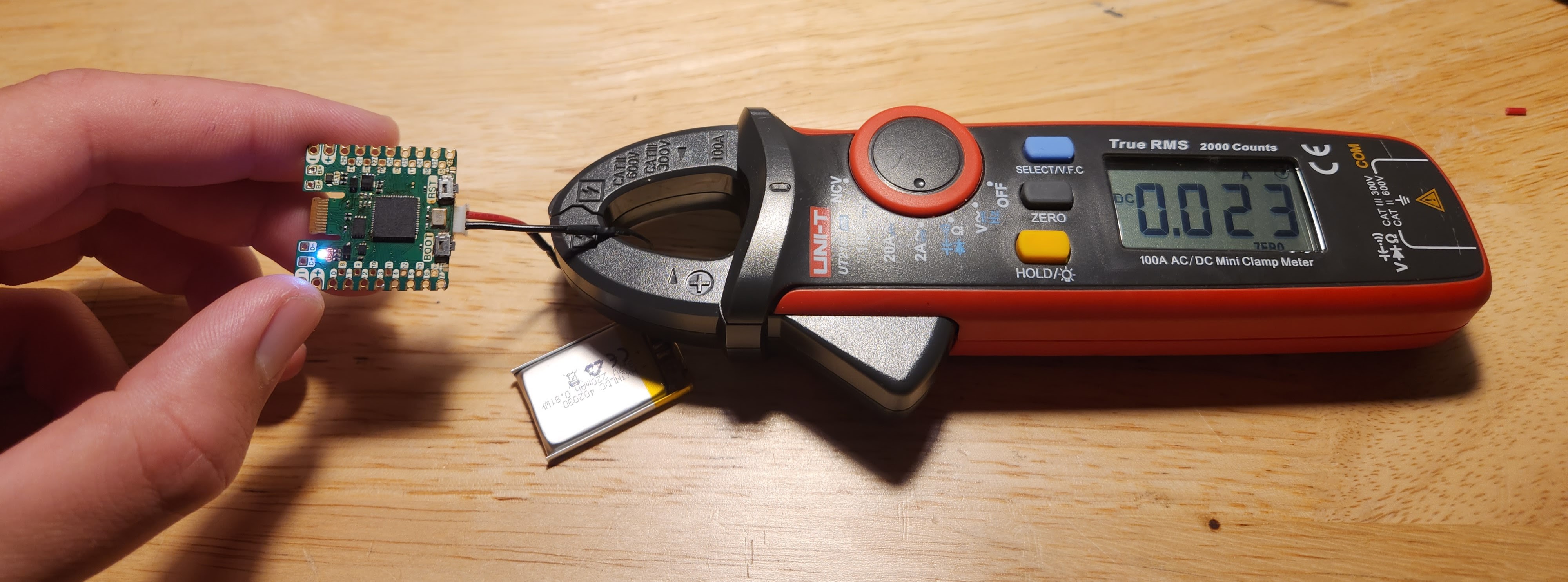
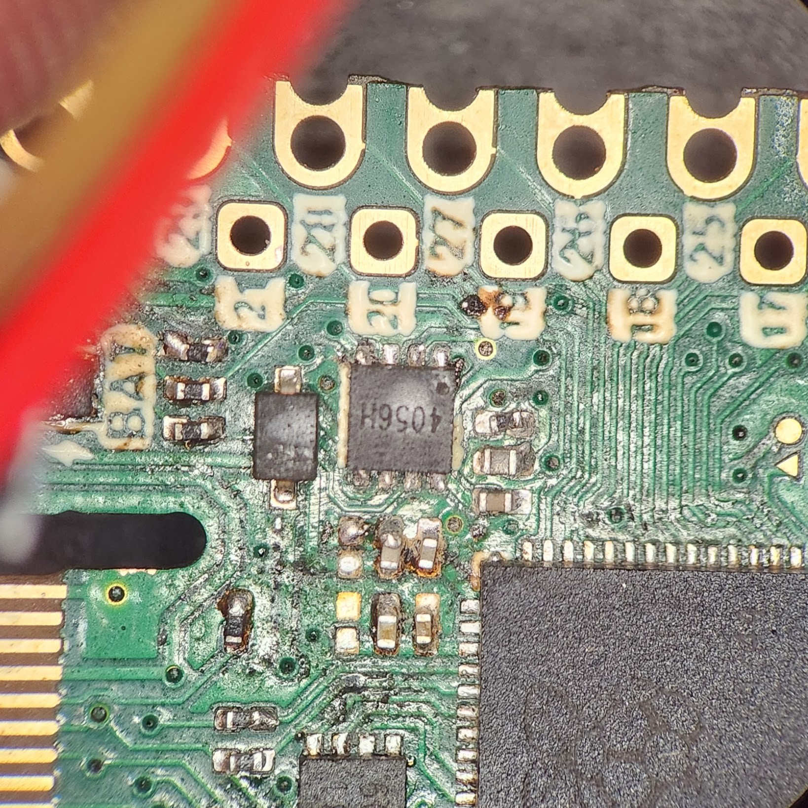
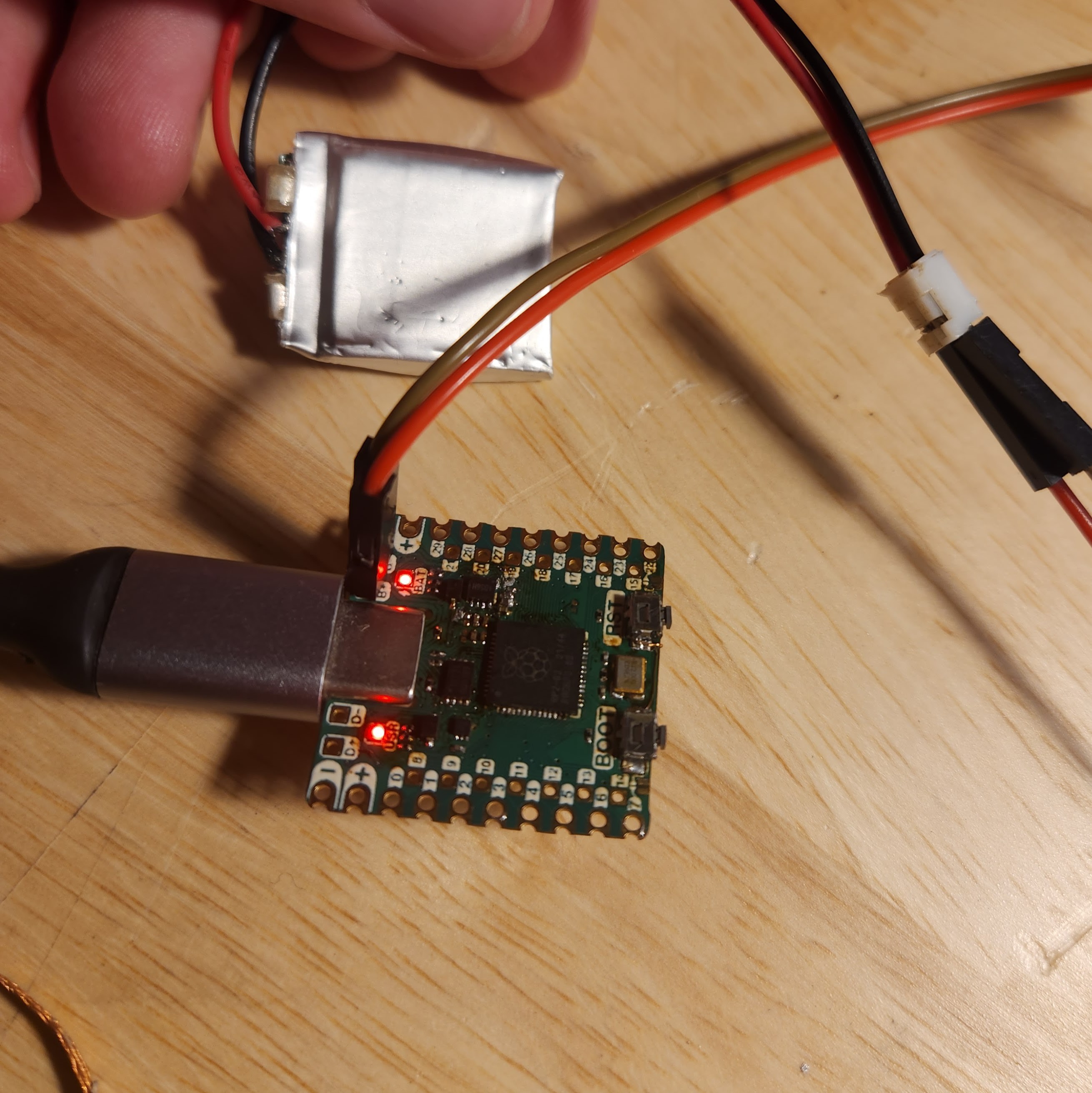
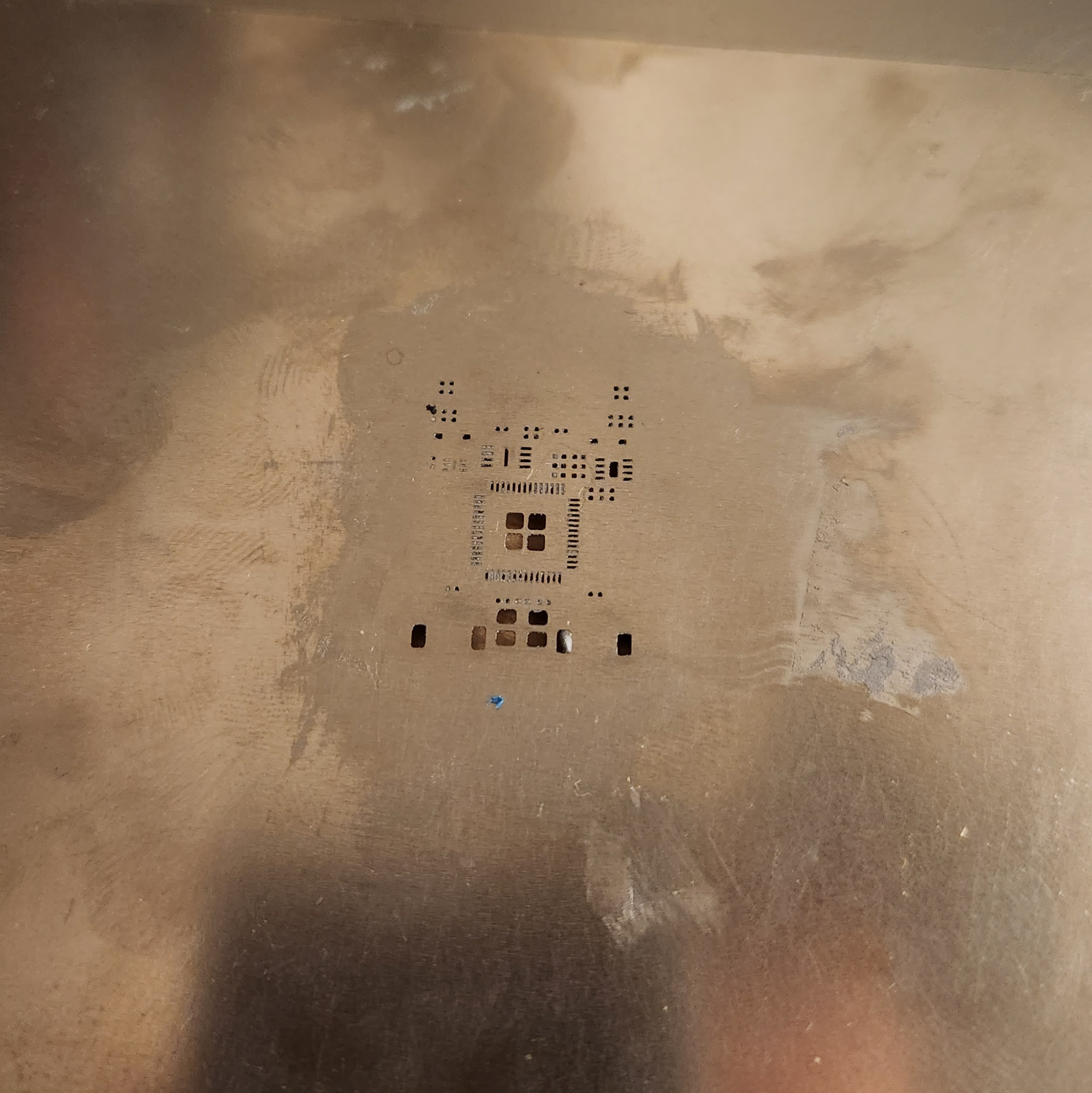
 The (G) stands for (G)old so it's cleare why ENIG would cost more money than HASL. When I sent the boards away I already knew that I was going to need to do another board revision so I didn't bother getting the good stuff. That turned out to be a great choice considering all the issues these boards would have. I'm not surprised, just disappointed.
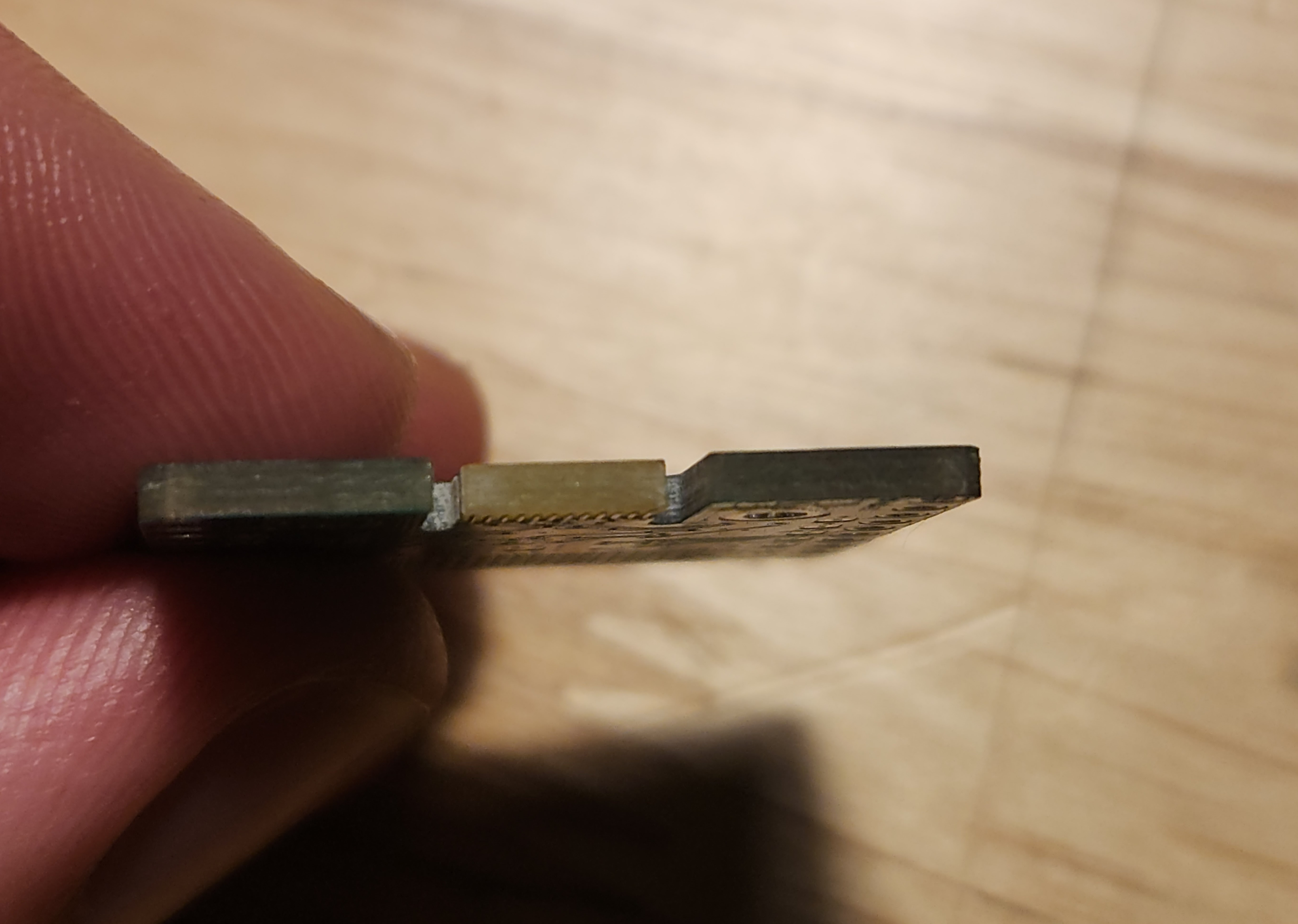


 Miroslav Zuzelka
 Jon Kunkee
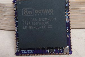
 Dylan Brophy
 Jeremy Gilbert
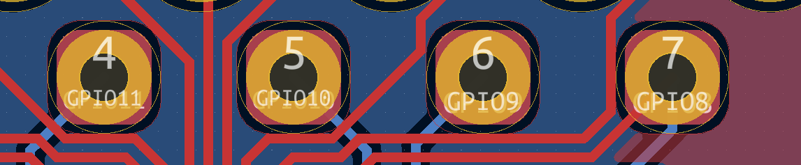
Interesting USB-C connector! Whats the BGA footprint on the rear for? I'm intrigued as the GPIO pins are consecutive - is this for PIO?